In today’s advanced materials and nanotechnology landscape, understanding a surface at the nanometer scale is critical. Whether it is a semiconductor chip, a graphene coating, a polymer film, or a biomedical sample, surface quality directly impacts performance. Atomic Force Microscopy (AFM) has emerged as one of the most powerful tools for nanoscale surface characterisation.
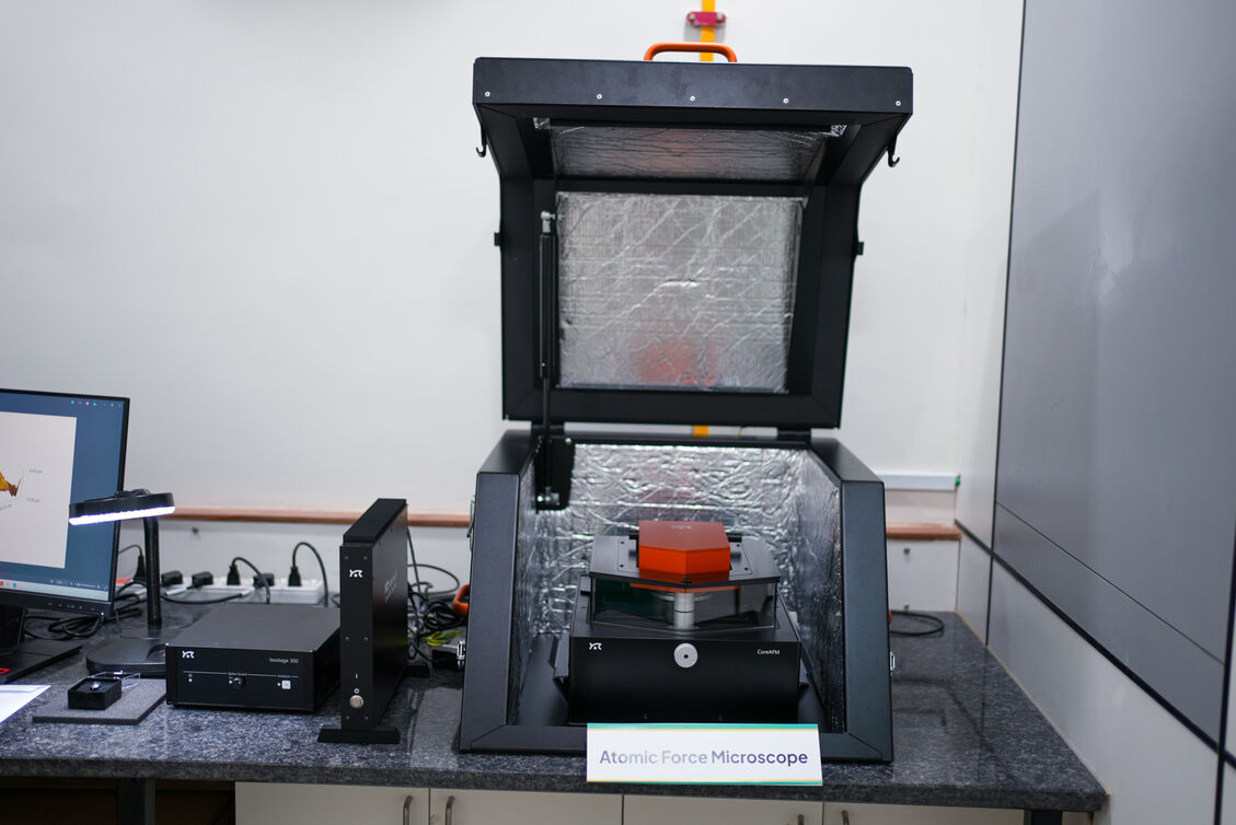
At the Micro–Nano Research & Development Centre (MNRDC), the Core AFM (imported from Switzerland, manufactured by NANOSURF AG) provides high-precision AFM testing services in Gujarat. With over 145 samples successfully analysed, the facility supports industries, researchers, and innovators requiring accurate nano-imaging and surface roughness analysis.
What is AFM? Why is it Important?
Atomic Force Microscopy allows scientists to see and measure surfaces at the atomic and nanometer level. Unlike optical microscopes that depend on light, AFM works like a highly sensitive “nano-finger” that physically feels the surface.
If XRD reveals what a material is made of internally, AFM reveals how the topmost surface layer looks and behaves. It helps determine:
- Surface roughness
- Nano-scale height variations
- Particle size and grain structure
- Mechanical, electrical, and magnetic properties (depending on mode)
This makes AFM essential for quality control, failure analysis, and advanced materials research.
The Science Behind AFM: How It Works
The Core AFM operates using a force-based principle.
At its heart is a tiny cantilever with an ultra-sharp tip (radius ~5–10 nm). As this tip scans across a surface:
The Cantilever Bends :
When the tip encounters microscopic bumps or valleys, the cantilever bends slightly.
Laser Reflection:
A 650 nm laser beam reflects off the cantilever.
Signal Detection:
A photodetector measures the laser’s movement, converting tiny deflections into precise height data.
This bending follows Hooke’s Law (F = −kx), where the cantilever behaves like a spring. The interaction between the tip and the sample is governed by Van der Waals forces, allowing the system to operate in contact, non-contact, or tapping modes.
The result is a true 3D nanoscale surface map.
AFM Modes for Surface Roughness & Nano Imaging
The Core AFM supports multiple imaging modes, but for most industrial and research applications, Tapping (Dynamic) Mode is preferred.
1. Contact Mode
The tip drags across the surface.
- Very high resolution
- May damage soft samples
2. Non-Contact Mode
The tip hovers above the surface without touching it.
- Ideal for delicate samples
3. Tapping Mode (Most Used)
The tip vibrates and gently taps the surface.
- Excellent for measuring surface roughness
- Suitable for thin films and coatings
For example, optical lenses are tested to ensure surface roughness remains below 100 nm to avoid irritation during use. Such roughness reports are crucial for verifying product quality.
Sample Types for AFM Testing
The AFM facility primarily handles solids and thin films, including:
- Graphene and nano-thin coatings
- Polymers
- Metals
- Semiconductors
- Biological samples
Loose powders can also be compacted into flat tablets to create a stable scanning surface.
Step-by-Step AFM Testing Process
The AFM testing procedure at the facility follows a systematic workflow :
1.Sample Mounting
The sample is placed on a flat stage.
2.Tip Approach:
The tip approaches the surface (approx. 5 minutes).
3.Scanning
A typical scan covers a 10 × 10 µm area with 256 lines at ~0.78 seconds per line.
4.Interaction:
The tip senses atomic-scale surface forces.
5.Signal Detection:
Laser-detected cantilever deflection is recorded.
6.Image Formation:
The system generates simultaneous 2D height, amplitude, and phase images.
Operators monitor live signal alignment to eliminate noise and ensure high-accuracy results.
Outputs Provided in AFM Testing
The facility provides:
- 2D Topography Images (colour-coded height maps)
- 3D Surface Images (mountain-like visualisation)
- Excel sheet with ISO-standard roughness values
- Roughness graphs and histograms
- Grain size distribution data
Using licensed MountainsSPIP software, over 50 ISO-standard surface roughness parameters (S-parameters) can be generated for detailed analysis.
Common measurements include:
- Surface roughness
- Step height
- Grain size
- Nano-indentation
- Adhesion and stiffness
Real-World Applications of AFM Testing in Gujarat
AFM testing plays a vital role across industries:
Electronics
Chip surface inspection and nano-coating verification
Pharmaceuticals
Tablet coating smoothness analysis for controlled drug dissolution
Polymers & Coatings
Surface uniformity and defect detection
Nanotechnology
Particle size mapping and nano-material characterisation
Energy Sector
Battery electrode surface analysis for performance optimisation
The Unique Superpower of AFM
One of the strongest advantages of AFM is its versatility. It can operate:
- In normal air
- Fully submerged in liquid
- Inside a vacuum chamber
This allows biological samples, polymers, and advanced coatings to be tested in their natural environment without damage.
Conclusion
Atomic Force Microscopy is more than just an imaging tool. It is a nano-scale measurement system that physically interacts with surfaces to generate precise, measurable data.
With its Swiss-imported Core AFM system, advanced imaging modes, ISO-standard roughness analysis, and detailed reporting capabilities, the AFM testing facility at MNRDC offers high-precision surface roughness and nano-imaging services in Gujarat.
For industries requiring nanoscale accuracy and reliable surface characterisation, AFM stands as one of the most powerful and indispensable analytical techniques available today.