Dr. Piyush S. Solanki is an Assistant Professor in the Department of Physics at Saurashtra University, Rajkot, and a member of the Functional Oxides Research Group – a research unit with a track record of publications in high-impact journals including Physica B, Ceramics International, Journal of Alloys and Compounds, and Materials Science in Semiconductor Processing.
Placing AFM in the Microscopy Landscape
Dr. Solanki opened by placing AFM within the full ecosystem of microscopy techniques. He presented the four major tool types – Atomic Force Microscopes (AFM), Transmission Electron Microscopes (TEM), Scanning Tunneling Microscopes (STM), and Scanning Electron Microscopes (SEM) – and established the framework distinguishing probe-based instruments (STM, AFM) from electron-based instruments (SEM, TEM).
This contextual framing helped participants who had spent the previous two days immersed in SEM to position AFM in relation to what they already knew. Access advanced nano research facilities at Parul University apply for 2026 programs today.
The Invention of AFM - 1986 and Its Significance
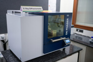
Dr. Solanki displayed an old photograph of this early device from the Science Museum Group collection – giving participants a concrete sense of how far the instrument has evolved in four decades, from this makeshift assembly to the precision Swiss-engineered Nanosurf Core AFM at the MNRDC.
How AFM Works - The Complete Principle
The fundamental operating principle of AFM, Dr. Solanki explained, is based on the interaction between the sample surface and a cantilever-tip assembly. As the probe raster-scans across the sample surface, atomic-scale forces cause the cantilever to deflect. A laser beam shines on the back of the cantilever. The reflected laser is caught by a Position-Sensitive Photo-Detector (PSPD).
The PSPD converts cantilever movement into electrical signals that are sent to a controller connected to a piezoscanner. The piezoscanner adjusts the sample’s position in real time to maintain a constant force on the sample. The scanner’s positional adjustments are combined with the scan position data to generate a three-dimensional surface map.
Dr. Solanki drew a complete schematic showing the laser source, mirror, PSPD, probe, sample, scanner, controller, and computer – illustrating how these components work together in a continuous feedback loop during every scan. Turn curiosity into innovation apply for Bachelor’s programs in nanotechnology at Parul University.
The Three AFM Imaging Modes - Explained With Diagrams
Dr. Solanki devoted significant time to explaining the three primary imaging modes using a force-distance curve diagram that showed where each mode operates along the interaction spectrum between tip and sample.
Contact Mode
In Contact Mode, the tip remains in continuous physical contact with the surface throughout the scan. It operates in the repulsive region of the force-distance curve, where tip and sample atoms push against each other. This mode delivers high resolution and is well suited for hard, robust samples such as metals and ceramics.
However, the lateral forces generated as the tip drags across the surface can damage soft samples – biological specimens and polymers – or wear out the tip rapidly. Researchers must evaluate whether their sample can withstand contact-mode forces before proceeding.
Tapping Mode (Intermittent Contact Mode)
Tapping Mode is the workhorse of modern AFM – the mode used most frequently at the MNRDC. The cantilever oscillates at its resonant frequency and makes contact with the surface only at the lowest point of each oscillation cycle, for an extremely brief duration. This intermittent contact strategy retains the high resolution of Contact Mode while dramatically reducing the lateral forces that cause sample damage.
Dr. Solanki showed animations demonstrating how the tip moves in Tapping Mode and used the force-distance diagram to indicate the transition zone where the tip alternates between attractive and repulsive force regimes.
Roughness parameters measured in Tapping Mode – Ra (average roughness) and Rq (RMS roughness) – were explained in terms of their physical meaning and how height distribution data is used to compute them.
WSxM Software Tutorial - From Raw Data to Published Results
The most practically distinctive portion of Dr. Solanki’s session was an extended live demonstration of WSxM 5.0 Develop software – a widely used open-source platform for scanning probe microscopy data analysis. Using raw data files from his own research at Saurashtra University, he walked participants through the complete analysis workflow from start to finish.
He demonstrated how to import raw scan data into WSxM, using the available processing options: Plane (to remove tilt from the scan), Flatten (to correct height offsets line by line), Derivative (to enhance edge detail), Reverse (to flip image orientation), and Equalize (to balance contrast). He showed the toolbar functions critical for quantitative analysis: Profile, Lattice, Mesh Average, and Roughness.
Participants were particularly struck by the ability to toggle between 2D and 3D visualisations of the same dataset – a top-down height map and a fully rendered three-dimensional terrain view with adjustable rotation angle, tilt, Z-scale, and lighting angle.
Dr. Solanki emphasised that a well-rendered 3D visualisation significantly strengthens the visual impact of AFM data in publications and presentations.
The Roughness Analysis demonstration used a real GCP-coated sample dataset, extracting RMS roughness (Rq = 29.15 nm in the example), average roughness (Ra), maximum peak-to-valley height, surface skewness, and surface kurtosis – all values directly referenced in peer-reviewed publications.
The Line Profile tool was used to draw a cross-section through the 2D image and extract a height-versus-distance profile for grain size measurement, with individual grain boundaries identified by peak analysis.
Dr. Solanki also demonstrated data export in multiple formats – bitmap, JPEG, ASCII matrix files, and 3D-printer-compatible STL files – emphasising the importance of saving both processed outputs and original raw STP files for research reproducibility.
Research From the Functional Oxides Lab, Saurashtra University
Dr. Solanki presented a comprehensive series of publications from his research group at Saurashtra University, demonstrating how AFM has been applied to complex oxide thin film systems. Materials studied include La-Pb-Mn-O (LPMO), La-Pr-Sr-Mn-O (LPSMO), Y-Sr-Mn-O (YSMO), Cdy-doped YMnO3, and LaMnO3/Nd-Sr-MnO3 interfaces at varying deposition thicknesses.
Publications appeared in Physica B, Ceramics International, Journal of Alloys and Compounds, and Materials Science in Semiconductor Processing.
In one study highlighted by Dr. Solanki, film thickness varied from 150 nm to 350 nm. The resulting changes in surface morphology and roughness – measured by AFM – directly correlated with the temperature of the metal-insulator transition for the material. This correlation between nanoscale surface data and macroscopic functional properties was cited by participants as a powerful demonstration of why surface characterisation matters beyond mere topography. Work with advanced instrumentation and nanoscale materials, apply for a Master of Science in Biotechnology at Parul University!
AFM Applications in Health Sciences - Directly Relevant for the Audience
Given that the workshop participants included pharmacy, Ayurveda, biotechnology, genetics, and medical researchers, Dr. Solanki devoted substantial time to health science applications of AFM – a departure from typical materials-focused AFM presentations.
- Cell Surface Imaging: AFM can image cancer cells, stem cells, neurons, and red and white blood cells in liquid environments that mimic physiological conditions – without the fixation and desiccation required for SEM. Images reveal cell shape, membrane surface roughness, and structural integrity at the nanoscale, complementing conventional light and electron microscopy.
- Cell Mechanics and Elasticity: Using force-distance curves and force-indentation measurements, AFM can measure the Young’s modulus of individual cells. Cancer cells have been shown to be measurably softer than healthy cells – a difference that has been investigated as an early diagnostic marker. Dr. Solanki cited published research on bladder cancer detection using this approach.
- Drug-Cell Interaction Studies: AFM is used to study how pharmaceutical compounds affect cell membranes and biomolecules at the molecular level. Structural changes in cells following drug administration, and the interaction of nanoparticle-based drug delivery systems with cell membranes, can be directly observed and measured.
AFM Applications in Nanotechnology and Materials Research
For nanotechnology applications, Dr. Solanki covered nanolithography – using the AFM tip as a nano-chisel to physically write patterns on surfaces with features smaller than what any optical technique can achieve – and PeakForce Quantitative Nanomechanical Mapping (PeakForce QNM), which simultaneously measures Young’s modulus, hardness, and adhesion forces at nanometre resolution.
These capabilities are essential for nanocomposites, flexible electronics, and MEMS/NEMS device characterisation.
In materials research, AFM enables thin film characterisation – thickness uniformity, surface defects, grain growth patterns – critical for solar cell development, gas sensors, and protective coatings. Lateral Force Microscopy (LFM), a specialised AFM mode, reveals friction differences between material phases, enabling phase identification in complex composite materials. Lead innovation in nanotechnology and pursue your Bachelors Science in Biotechnology & Masters Science in Biotechnology at Parul University for 2026 admissions
FAQs
What is WSxM software and how is it used for AFM data analysis?
WSxM 5.0 Develop is a free, widely used software for analysing scanning probe microscopy data. It converts raw AFM scan files into processable images, enables height data correction (plane levelling, line-by-line flattening), generates 2D and 3D visualisations, extracts quantitative roughness parameters (Ra, Rq, Rz, skewness, kurtosis), performs grain size analysis via line profiles, and exports data in formats suitable for publication - including JPEG, ASCII, and 3D-printer-compatible STL files.
How is AFM used in health sciences and pharmaceutical research?
AFM is used in health sciences for imaging cell surfaces (cancer cells, stem cells, blood cells) in near-physiological liquid environments; measuring cell stiffness (Young's modulus) using force-indentation curves - with cancer cells measurably softer than normal cells; studying drug-cell membrane interactions at the molecular level; characterising pharmaceutical tablet surfaces for roughness and uniformity; and characterising nanoparticle-based drug delivery systems.