What Is Atomic Force Microscopy?
Atomic Force Microscopy (AFM) is a surface analysis technique that works by touch rather than sight. While most microscopes use light or electrons to “see” a surface, AFM uses a physical probe an ultra-sharp tip attached to a flexible cantilever to “feel” the surface at atomic resolution. As the tip scans the surface atom by atom, the cantilever bends in response to the forces it encounters. These deflections are measured with nanometre precision and converted into a three-dimensional map of the surface topology.
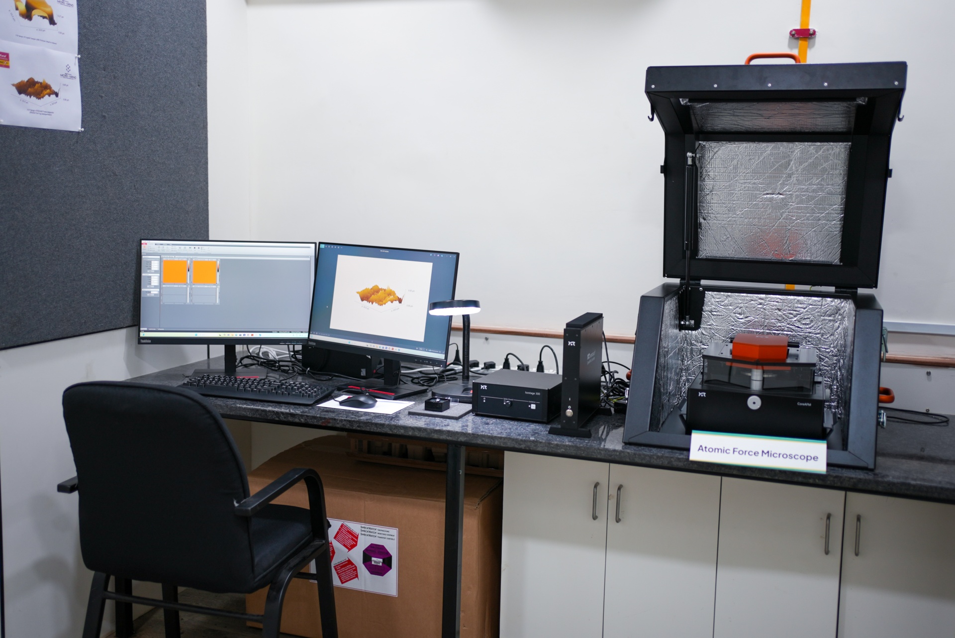
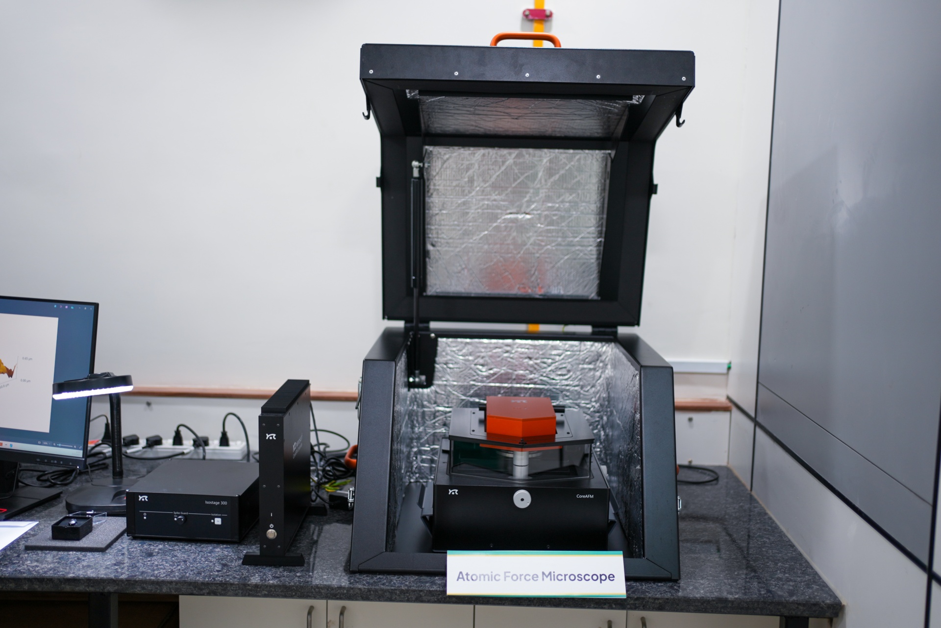
The Nanosurf Core AFM at the MNRDC, manufactured by NANOSURF AG, Switzerland (a global leader in AFM instrumentation) and installed in 2024 at ₹76 lakh, has characterised over 145 samples across thin films, polymers, metals, semiconductors, and biological specimens. It represents one of the most capable surface analysis tools available at any Indian university research centre.
The Physics of AFM - Hooke's Law and Van der Waals Forces
Two fundamental physical laws govern AFM operation. Hooke’s Law (F = kx) describes the cantilever’s behaviour: it acts exactly like a spring. When the tip encounters a surface feature, the cantilever deflects by a distance x. By knowing the cantilever’s spring constant k, the force F causing the deflection can be precisely calculated. The cantilever’s spring constant is a key specification the Nanosurf Core AFM uses a Dyna190 Al tip with a spring constant of 48 N/m, aluminium-coated for efficient laser reflection.
Van der Waals forces the weak, short-range attractive and repulsive forces between all atoms when they are in close proximity provide the actual “signal” that the AFM detects. At a slight distance from the surface, the tip atoms are attracted to the sample atoms (attractive Van der Waals regime). When the tip comes into contact, the overlapping electron clouds of tip and sample atoms repel each other (repulsive regime). AFM modes are defined by which regime of the Van der Waals interaction they exploit.
The Laser Detection System - How Deflection Becomes Data
A 650nm laser beam is focused on the back of the aluminium-coated cantilever. When the cantilever deflects up, down, or sideways the laser beam reflects at a different angle. This reflected beam falls on a Position-Sensitive Photo-Detector (PSPD) that measures the exact position of the reflected spot with nanometre precision. The PSPD converts the reflected laser position into an electrical signal that is fed into the controller. The controller drives a piezo scanner a device that moves with sub-nanometre precision to adjust the tip-to-sample distance, maintaining a constant setpoint (either constant force in Contact Mode or constant oscillation amplitude in Tapping Mode). The combination of scan position data and piezoscanner height adjustments generates the three-dimensional surface map.
Two manual knobs control the X and Y position of the laser on the cantilever back. Correct laser alignment centred precisely on the cantilever tip is verified through two camera views: a top view showing the laser spot position relative to the cantilever, and a side view showing the cantilever and its reflection in the sample surface as the tip approaches. Correct alignment before scanning is critical; misalignment prevents any signal from being generated. Build a strong foundation in biotech with Parul University’s B.Sc. programme.
AFM Imaging Modes - Contact, Non-Contact, and Tapping
Contact Mode operates in the repulsive regime: the tip is in continuous physical contact with the surface as it scans. This delivers the highest resolution and is appropriate for hard, robust materials metals, ceramics, and hard polymers. The limitation is the lateral dragging force generated as the tip moves across the surface, which can scratch soft samples or degrade biological specimens. Contact Mode is not suitable for soft materials.
NonContact Mode operates in the attractive regime: the cantilever oscillates at its resonant frequency near but not touching the surface. The instrument monitors changes in oscillation frequency caused by the attractive forces from the surface. This completely avoids physical contact, preserving delicate samples. The tradeoff is lower resolution and susceptibility to interference from ambient humidity and vibration, making controlled environments important.
Tapping Mode (Dynamic Mode or Intermittent Contact Mode) is the most widely used mode at the MNRDC. The cantilever oscillates at its resonant frequency and taps the surface briefly at the lowest point of each oscillation making and breaking contact hundreds of thousands of times per second. This eliminates the lateral dragging forces of Contact Mode while maintaining resolution approaching Contact Mode quality. Tapping Mode is appropriate for soft materials including biological samples, polymers, and nanofibre specimens. At the MNRDC, optical lenses are verified using Tapping Mode to confirm their surface roughness is below 100nm roughness above this threshold would cause eye irritation in contact lens applications.
Advanced AFM Modes - Magnetic, Electrical, and Mechanical
Beyond the three primary imaging modes, AFM offers specialised capabilities. Magnetic Force Microscopy (MFM) uses a cobalt coated tip to map magnetic domain structures relevant for hard disk research, MRAM development, and spintronics. Electrical Force Microscopy (EFM) applies a voltage to the tip to detect electrical charge distributions on semiconductor and polymer surfaces. Conductive AFM (CAFM) maps electrical conductivity across a surface. Kelvin Probe Force Microscopy (KPFM) measures surface potential distributions. Piezoresponse Force Microscopy (PFM) images ferroelectric domain structures in piezoelectric materials.
Mechanical property modes include Force Modulation (mapping stiffness by wiggling the tip while in contact) and Force Spectroscopy (force distance curves that measure adhesion and elasticity at a single point). PeakForce Quantitative Nanomechanical Mapping simultaneously measures Young’s modulus, adhesion, and deformation across the full scan area.
The Scan Process - Step by Step at the MNRDC
A standard AFM scan at the MNRDC covers a 10 × 10 µm area at a resolution of 256 lines meaning the tip makes 256 horizontal passes from top to bottom. Each line is scanned at 0.78 seconds per line, a speed chosen to balance detail capture against thermal drift (where temperature fluctuations cause image distortion during longer scans). Total scan time for a standard image is approximately 3–4 minutes.
Samples for AFM must be solid, with a maximum size of 10mm × 10mm × 7mm. Powder samples can be compacted into flat pellets to create a scannable solid surface. The MNRDC provides each user with a 2D height image, a 3D surface render, an Excel sheet of roughness values, and a roughness graph as standard output. Delay no more & deepen your expertise with Parul University’s Master of Science in Biotechnology.
MountainsSPIP Software - From Raw Data to Published Results
The MNRDC uses MountainsSPIP commercial software for AFM data analysis. Like WSxM, it converts raw scan data into processable images but with over 50 ISO standard surface roughness parameters (S parameters) available for areal surface analysis. MountainsSPIP generates complete roughness reports covering Ra, Rq, Rz, Sa, Sq, skewness, kurtosis, and maximum peak to valley height with one click, producing figures directly usable in peer reviewed publications. It also generates grain size histograms (threshold grain graphs) that measure and count individual surface grains, providing particle size distribution data from AFM scans.
Career in Nanotechnology After 12th - Why Instrument Access Matters
For students considering a career in nanotechnology, materials science, or nanomedicine after 12th standard, the question of research infrastructure is not abstract it directly determines the quality of education and the speed of career development. A nanotechnology degree programme that provides access to actual instruments SEM, XRD, AFM from the beginning of a student’s research journey creates a fundamentally different graduate than a programme that covers the same topics theoretically.
At Parul University, students from engineering, pharmacy, biotechnology, and applied sciences have direct access to MNRDC’s 10 instrument facility, with applications open for 2026 admissions. PhD scholars like Srishti Rawal, who uses SEM for her heterogeneous catalyst doctoral research, and Moutughimou Ben Ali, a genetics PhD student who gained direct hands on AFM experience, represent the kind of research capable graduates that universities with genuine infrastructure produce.
Career pathways from nanotechnology and materials science include research scientist roles in semiconductor companies (Qualcomm, Samsung, Intel), pharmaceutical development positions focusing on nanoparticle drug delivery, aerospace materials engineering at organisations like ISRO and DRDO, battery technology research for electric vehicle companies, academic research and faculty positions, and materials testing and quality assurance roles across manufacturing industries. Starting salaries for nanotechnology graduates in India range from ₹4–8 lakh per annum for entry level industry roles, scaling significantly with experience and research output.
AFM Applications at the MNRDC - What Researchers Use It For
The MNRDC’s AFM is used across a wide range of research applications. Pharmaceutical tablet and nanoparticle surface characterisation confirming coating smoothness and uniformity. Thin film surface topography for solar cell research, sensor fabrication, and semiconductor applications. Biological sample imaging cell membranes, protein assemblies, and DNA in liquid environments. Polymer surface analysis roughness, grain structure, and phase distribution. Nanocomposite characterisation particle size, distribution, and surface interaction. Optical lens and precision surface quality control verifying roughness below application specific thresholds.
FAQ
What is the AFM at Parul University MNRDC?
The MNRDC at Parul University operates a Nanosurf Core AFM manufactured by NANOSURF AG, Switzerland, installed in 2024 at a cost of ₹76 lakh. It uses a Dyna190 Al tip with a spring constant of 48 N/m, operates in Contact, Non-Contact, and Tapping modes, scans areas up to 10×10 µm at 256-line resolution, and provides 2D images, 3D surface renders, and roughness parameter reports. Over 145 samples have been analysed to date.
What career options are available after studying nanotechnology in India?
Nanotechnology graduates in India can pursue careers as research scientists in semiconductor and electronics companies, pharmaceutical development specialists focused on nanoparticle drug delivery, aerospace materials engineers at ISRO or DRDO, battery technology researchers for EV companies, academic researchers and faculty, and materials testing specialists in manufacturing quality assurance. Entry-level salaries range from ₹4–8 lakh per annum, with significant growth potential for those with strong research output and instrument proficiency.
Can AFM be used on biological samples?
Yes. AFM can image biological samples - cells, bacteria, DNA strands, proteins - in liquid environments that mimic physiological conditions, without the fixation, desiccation, and gold coating required for SEM. It can also measure the mechanical stiffness (Young's modulus) of individual cells using force-distance curves - a technique that has been used to distinguish cancer cells from healthy cells, since cancer cells are measurably softer.
What surface roughness parameters does AFM measure?
AFM measures Ra (arithmetic average roughness), Rq or RMS roughness, Rz (maximum peak-to-valley height), and their areal equivalents Sa and Sq. MountainsSPIP software generates over 50 ISO-standard surface parameters automatically. Additional statistical descriptors from height distribution histograms include skewness (surface asymmetry) and kurtosis (sharpness of the height distribution). Grain size and particle size distributions are also extractable from AFM scan data.