Advanced material characterisation tools are often described in terms of extreme precision: microns, nanometres, atomic layers. However, every instrument has practical limits shaped by physics, sample preparation, detector capability, and operational settings. Understanding these limits is essential for choosing the right technique and interpreting results correctly.
This article explains the practical resolution boundaries of Scanning Electron Microscopy (SEM), Atomic Force Microscopy (AFM), and X-Ray Diffraction (XRD), based on real operational parameters and instrument behaviour.
SEM Resolution: How Fine Can Surface Imaging Go?
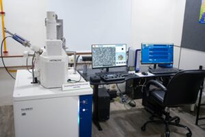
Scanning Electron Microscopy is widely used for surface morphology analysis, examining structure, particle size, and distribution. While SEM is known for high magnification, its practical resolution depends on accelerating voltage, working distance, detector sensitivity, and sample conductivity.
In standard operation, images are measured in microns (µm), with common resolution scales such as 30 µm, 10 µm, and 5 µm. These scales reflect practical imaging fields during routine analysis. Although SEM systems can theoretically achieve nanometre-scale resolution, real-world imaging must balance clarity and sample stability.
Voltage Limits and Sample Damage
Power settings directly influence resolution. For solid samples, voltage typically ranges from 5–30 kV, while liquids and semi-solids are restricted to 3–15 kV. Higher voltage improves image sharpness by increasing beam penetration and signal generation. However, excessive power can damage sensitive samples, particularly liquids.
Thus, practical SEM resolution is often limited not by the machine itself, but by the material being studied.
Sample Preparation as a Limiting Factor
Non-conductive samples require gold coating to prevent charging. Improper coating thickness can reduce clarity or mask fine surface details. Working distance also plays a role: SEM imaging typically operates at around 5 mm, while EDS operates at 10 mm. Increasing working distance improves safety and stability but slightly reduces resolution.
In practice, SEM delivers reliable micro-to-submicron surface imaging, but surface conductivity, coating thickness, and beam energy define its real limits.
AFM Nanoscale Imaging: Touching the Atomic Landscape
Atomic Force Microscopy operates differently from SEM. Instead of using electrons, it “feels” the surface with an ultra-sharp tip attached to a cantilever. AFM measures nanoscale height variations, surface roughness, and particle morphology.
True Nanoscale Capability
AFM is capable of atomic and nanometre-scale measurements because it detects physical forces between the tip and surface. The cantilever follows Hooke’s Law (F = –kx), converting minute deflections into measurable force data. This allows vertical resolution down to fractions of a nanometre under optimal conditions.
However, lateral resolution is limited by the tip radius, typically 5–10 nm. A blunt or worn tip reduces sharpness, making nanoscale grain boundaries appear broader than they actually are.
Scan Area and Resolution Trade-Off
In routine operation, AFM scans a 10 × 10 µm area with a resolution of 256 lines. Increasing scan area reduces nanoscale detail, while increasing resolution slows scanning and increases drift risk.
Scan speed also matters. Each line is scanned at approximately 0.78 seconds per line. Faster scanning can cause tip “flight” over fine features, while slower scanning increases thermal drift, leading to image distortion.
Environmental Sensitivity
AFM can operate in air, in liquids, or in a vacuum. However, vibrations, temperature changes, and contamination strongly affect nanoscale accuracy. Even minor external disturbances can influence cantilever response.
In practical terms, AFM achieves true nanoscale vertical precision, but tip condition, scan parameters, and environmental control define its real imaging limits.
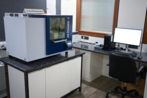
XRD Precision: Atomic Structure Without Imaging
X-Ray Diffraction does not produce surface images. Instead, it reveals internal crystal structure using Bragg’s Law (nλ = 2d sinθ). X-rays are chosen because their wavelength (~0.1 nm) matches atomic spacing, enabling atomic-level structural analysis.
Angular Precision and Detector Technology
XRD precision depends on angular measurement accuracy and detector sensitivity. Modern systems use a Position Sensitive Detector (PSD), such as the LYNXEYE XE-T, which captures multiple angles simultaneously. This enables faster scans with sharp diffraction peaks.
Older point detectors measured one angle at a time, increasing scan duration and noise. Continuous PSD fast mode reduces scan time while preserving peak resolution.
Practical Limits in Interpretation
XRD graphs typically use a 10°–80° (2θ) range, where most characteristic peaks appear. Peak width indicates crystallite size, and peak shifts reveal internal stress.
However, precision depends on sample preparation. Improper flattening or uneven surfaces affect peak intensity. Additionally, thin coatings may require Grazing Incidence XRD to prevent signal dominance from the substrate.
Unlike SEM or AFM, XRD does not provide spatial resolution. Its precision lies in phase identification and lattice parameter measurement rather than imaging.
Comparing Practical Limits
Each instrument excels in a specific domain:
- SEM provides high-resolution surface morphology but is limited by beam interaction and sample conductivity.
- AFM offers true nanoscale height measurement but depends on tip sharpness and environmental stability.
- XRD delivers atomic structural precision but lacks spatial imaging capability.
SEM shows what the surface looks like. AFM measures how rough or smooth it truly is at the nanometre scale. XRD reveals how atoms are arranged internally.
Conclusion
Resolution is not just about the smallest number an instrument can theoretically measure. It is about reliable, repeatable performance under real laboratory conditions.
SEM balances beam energy and sample stability to achieve micro-to-submicron imaging. AFM achieves nanometre- and sub-nanometre-level vertical precision but depends heavily on tip and vibration control. XRD achieves atomic structural precision through angular measurement and diffraction physics.
Understanding these practical limits ensures that researchers choose the right tool for the right question and interpret results with scientific confidence.