Start Here: What Are You Trying to Find Out?
Material characterisation is not about running the most tests – it is about running the right test for the question you are asking. Every instrument at the MNRDC answers a different class of questions. Identify which of the following questions your research is asking, and the correct instrument follows directly.
Question 1: What Does the Surface of My Material Look Like?
Answer: SEM + EDS - Hitachi SU3800 - 897+ Samples Analysed
Use SEM when you need to see surface morphology – grain structure, particle size and shape, surface defects, fracture patterns, coating uniformity, or phase distribution – at resolutions down to approximately 3-4 nm. Add EDS in the same session to determine elemental composition: which elements are present, in what proportions, and where they are distributed spatially (area mapping). Standard output: 8 SEM images + 2 EDS spectra + area mapping on request. Turnaround: 10 days standard, 1 day urgent (4 images).
Use SEM for: pharmaceutical powder particle morphology, nanoparticle synthesis verification, fracture surface analysis, grain size in metals and alloys, nanowire and nanotube imaging, biological specimen imaging (tissues, cells, bacteria), semiconductor defect inspection, geological mineral characterisation, industrial wear track analysis, and coating uniformity verification. Sample requirement: solid (or dried liquid), maximum 100mm diameter × 50mm height.
Question 2: What Crystal Structure Is My Material and Which Phases Does It Contain?
Answer: XRD - Bruker D6 PHASER - 600+ Samples Analysed
Use XRD when you need to identify crystalline phases, measure crystallite size, detect lattice strain, or quantify phase proportions in a mixture. The D6 PHASER uses Bragg’s Law (nλ = 2d sinθ) to generate a unique diffraction fingerprint matched against the ICDD PDF-4 database (1 million+ reference patterns). TOPAS Rietveld refinement provides quantitative phase analysis. Add GIXRD (on request) for thin film surface-sensitive analysis. Add XRR (on request) for thin film thickness (1-500nm), surface roughness, and density.
Use XRD for: drug polymorph identification in pharmaceutical development, heat treatment outcome verification in metals (austenite-to-martensite transformation), battery electrode composition confirmation, residual stress measurement in engineered components, synthesised material structure confirmation, cement phase analysis in construction materials, forensic powder identification, and semiconductor layer crystal quality verification. Sample requirement: powder (minimum 800mg finely ground) or solid (maximum 30mm diameter × 5mm thickness).
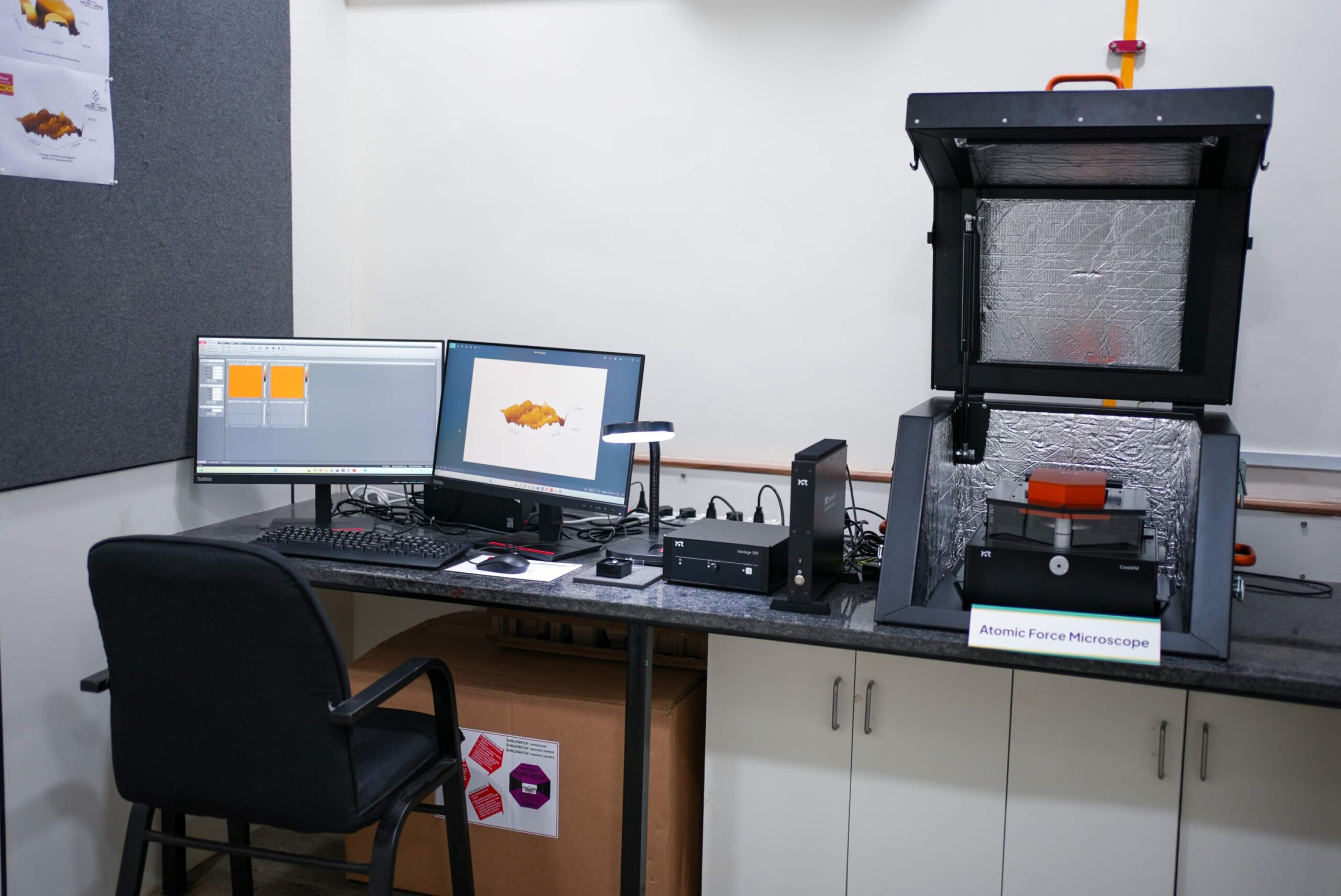
Question 3: How Rough or Smooth Is My Surface at the Nanoscale?
Answer: AFM - Nanosurf Core - 145+ Samples Analysed
Use AFM when you need quantitative nanoscale surface topography – roughness parameters (Ra, Rq, Rz and 50+ ISO S-parameters via MountainsSPIP), 3D surface maps, or grain size at the nanoscale. The Core AFM operates in air, liquid, or vacuum, making it unique for biological sample imaging in physiological conditions. Standard output: 2D image, 3D surface render, Excel roughness data, roughness graph. Tapping Mode is the default – gentle enough for soft and biological samples while delivering high resolution.
Use AFM for: optical lens surface roughness verification (must be below 100nm), thin film quality characterisation after sputtering deposition, pharmaceutical tablet coating roughness, nanoparticle morphology at sub-100nm scale, biological cell surface imaging in liquid, DNA and protein imaging, grain size analysis of nanostructured coatings, and ferroelectric domain imaging (PFM mode). Sample requirement: solid or compacted powder pellet, maximum 10mm × 10mm × 7mm.
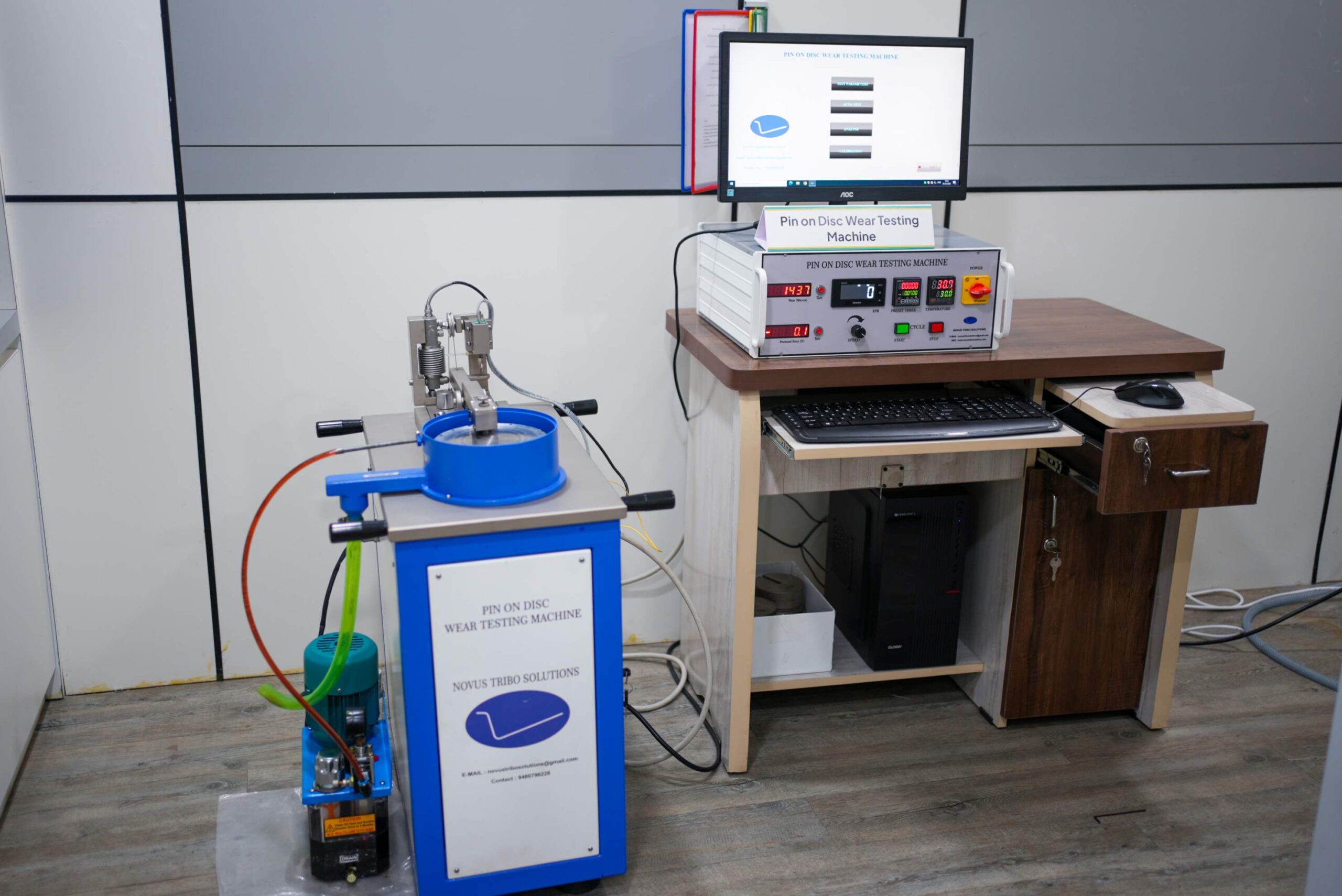
Question 4: How Does My Material Perform Under Friction and Wear?
Answer: Pin-on-Disc Tribometer - NTS-R&D-03 - 118+ Specimens Tested
Use the Tribometer when you need wear rate, coefficient of friction (COF), or material durability data under sliding contact – the information that predicts component lifetime in service. The MNRDC operates to ASTM G99 standard, the internationally recognised protocol for Pin-on-Disc wear testing. Three test modes: dry (no lubrication), lubricated (submerged in oil, water, or process fluid), and heated (pin at elevated temperature). Standard output: Excel file with time-resolved friction force, COF, sliding distance, and calculated wear rate.
Use the Tribometer for: brake pad material evaluation, bearing alloy screening, polymer joint material for medical implants (UHMWPE hip/knee), cutting tool coating performance, floor material wear resistance, gear material selection, and comparing new materials against existing specifications. Combine with SEM after tribometer testing to examine worn surfaces and identify the wear mechanism. Sample requirement: cylindrical solid pin, 6-12mm diameter, 25-30mm length.
Question 5: What Are the Electrical or Dielectric Properties of My Material?
Answer: LCR Meter ZM2376 - NF Corporation Japan - 61+ Samples Analysed
Use the LCR Meter when you need resistance, capacitance, inductance, impedance, quality factor (Q), dissipation factor (D), or dielectric permittivity – measured across a continuous frequency sweep from 1 mHz to 5 MHz. The ZM2376’s defining capability is frequency-dependent characterisation: revealing how a material’s electrical behaviour changes with frequency, which is impossible to determine from single-frequency measurements. High-temperature testing is available up to 1200°C via an integrated furnace with gold-plated electrodes.
Use the LCR Meter for: ceramic capacitor dielectric characterisation, polymer dielectric property evaluation for flexible electronics, battery electrode material electrical characterisation, electronic component testing, sensor material evaluation, and temperature-dependent impedance spectroscopy of advanced ceramics. Sample requirement: solid only (powders compacted into pellets), approximately 10-20mm diameter.
.
Question 6: I Need to Deposit a Thin Film - What Do I Need?
Answer: RF/DC Magnetron Sputtering Auto 500 - HHV India - 22 Runs Completed
Use sputtering when you need to coat a substrate with a thin film – metals, oxides, nitrides, or organic compounds – with precise control over thickness, composition, and crystal structure. The Auto 500 combines three methods: DC sputtering (conductive materials: Ti, Mo, Cr, Al, Au), RF sputtering (insulators and oxides: SiO2, Al2O3, ITO, TiO2, TiN), and thermal evaporation (soft metals and organics). Substrate heating to 600°C and rotation to 20 RPM ensure uniform, well-adhering films. After deposition, verify film quality with XRR (thickness and roughness), XRD or GIXRD (crystal structure), and SEM (surface morphology).
Use sputtering for: solar cell test structure fabrication (Mo back contact + buffer + ITO front electrode), hard TiN coatings on cutting tools and medical implants, transparent conducting ITO films, metamaterial antenna substrate preparation, semiconductor device layer deposition, anti-reflective optical coatings, and biocompatible surface coatings on medical implants.
Combination Strategies - Multi-Instrument Workflows at the MNRDC
For pharmaceutical development
XRD (polymorph identification and crystal structure) + SEM+EDS (particle morphology and elemental verification) + AFM (tablet coating surface roughness) + DSC/incoming (thermal analysis, melting point, glass transition, excipient compatibility).
For failure analysis of a mechanical component
SEM (fracture surface morphology and features) + XRD (phase identification – was the heat treatment correct?) + Tribometer (wear rate of the material in question) + EDS (contamination or composition shifts at the fracture).
For new thin film or coating research
Sputtering (deposit film) + XRR (measure thickness and surface roughness) + GIXRD (crystal structure of the film) + AFM (nanoscale surface topography) + SEM (cross-sectional imaging of film on substrate).
For metal matrix composite development
Stir Casting (fabricate MMC) + SEM+EDS (reinforcement particle distribution and composition) + XRD (phase identification in matrix and reinforcement) + Tribometer (wear resistance of the composite vs unreinforced matrix).
The MNRDC’s integrated portfolio makes multi-instrument workflows practical – 10 instruments under one roof, 10-day standard turnaround, no coordination overhead across multiple external facilities. Submit your sample and research question and the research cadre will advise on the optimal testing sequence.
Quick Reference - Instrument Selection at a Glance
- Surface morphology, grain structure, and particle size/shape analysis is carried out using SEM along with EDS for elemental composition.
-
- Crystal structure, phase identification, and polymorph confirmation are performed using XRD techniques.
-
- GIXRD is used for thin film analysis.
- XRR helps determine film thickness, roughness, and density.
-
- Crystal structure, phase identification, and polymorph confirmation are performed using XRD techniques.
- Nanoscale roughness parameters such as Ra, Rq, and Rz, along with 3D surface topography and grain size, are analyzed using AFM.
- Wear rate, friction coefficient, and material durability under sliding conditions are evaluated using a Pin-on-Disc Tribometer following ASTM G99 standards.
- Electrical and dielectric properties, including frequency-dependent behavior and impedance, are measured using the LCR Meter ZM2376.
- Thin film deposition of metals, oxides, nitrides, and organic materials is carried out using RF/DC Magnetron Sputtering Auto 500.
- Thermal phase transitions such as melting point, glass transition, and enthalpy are analyzed using DSC NEXTA 200.
- Simultaneous heat flow and mass change, including decomposition temperature, are measured using STA NEXTA 200.
- Cutting force measurement during machining is performed using a piezo-based dynamometer.
- Precision micro-machining of small components or specimens is achieved using CNC Hyper-15.
- Metal matrix composite fabrication under controlled conditions is done using a stir casting machine.
- ASTM-standard polymer and composite test specimens are prepared using a compression molding machine.
FAQs
What is the difference between SEM and XRD for material characterisation?
SEM images the surface morphology of a material - shape, texture, grain structure, particle distribution. It shows what the surface looks like. XRD reveals the internal crystal structure - atomic arrangement, crystalline phases, crystallite size, and lattice strain. It reveals what the material is and how it is structured inside. They are complementary and frequently used together: SEM shows appearance, XRD confirms identity and phase. Both are available at the MNRDC.
When should I use AFM instead of SEM?
Choose AFM when you need quantitative nanoscale roughness parameters (Ra, Rq, Rz, 50+ S-parameters), 3D surface topography at nanometre precision, characterisation of non-conductive samples without coating, imaging in liquid environments (biological samples), or surface mapping below 100nm features. Choose SEM for larger-area morphology surveys, when EDS elemental analysis is needed, or for features at the micrometre scale and above. For comprehensive surface characterisation, use both.
Can I combine multiple tests on the same sample at Parul University MNRDC?
Yes. All MNRDC characterisation tests (SEM+EDS, XRD, AFM, LCR Meter) are non-destructive - samples emerge in the same condition they entered. The Tribometer involves sliding wear and is inherently destructive of the contact surface. You can request SEM+XRD+AFM in a single sample submission for multi-parameter characterisation. Contact micronanornd.paruluniversity.ac.in to discuss the optimal test sequence for your sample and research question.
Which test should I use for pharmaceutical particle characterisation?
For pharmaceutical samples: use XRD to identify drug polymorphs and confirm crystal structure. Use SEM+EDS to characterise API particle size, shape, and elemental composition. Use AFM to measure tablet coating surface roughness. Use the LCR Meter for dielectric properties of polymer excipients. Use DSC (Hitachi NEXTA, incoming) for thermal analysis, melting point, glass transition, and excipient compatibility screening. Contact the MNRDC research cadre for guidance specific to your formulation.