Thin film deposition is the controlled growth of material layers – from a few nanometres to several micrometres thick – onto a substrate surface. These films are the foundation of modern electronics (every transistor and interconnect in a microchip is a thin film), photovoltaics (solar cell absorber and contact layers), hard coatings (the wear-resistant surface on cutting tools and medical implants), optical coatings (anti-reflective layers on camera lenses and glasses), and sensors (thin film pressure, gas, and biosensors). To give perspective: a human hair is approximately 80,000 nanometres wide. The films deposited by the MNRDC’s sputtering system are measured in nanometres to hundreds of nanometres.
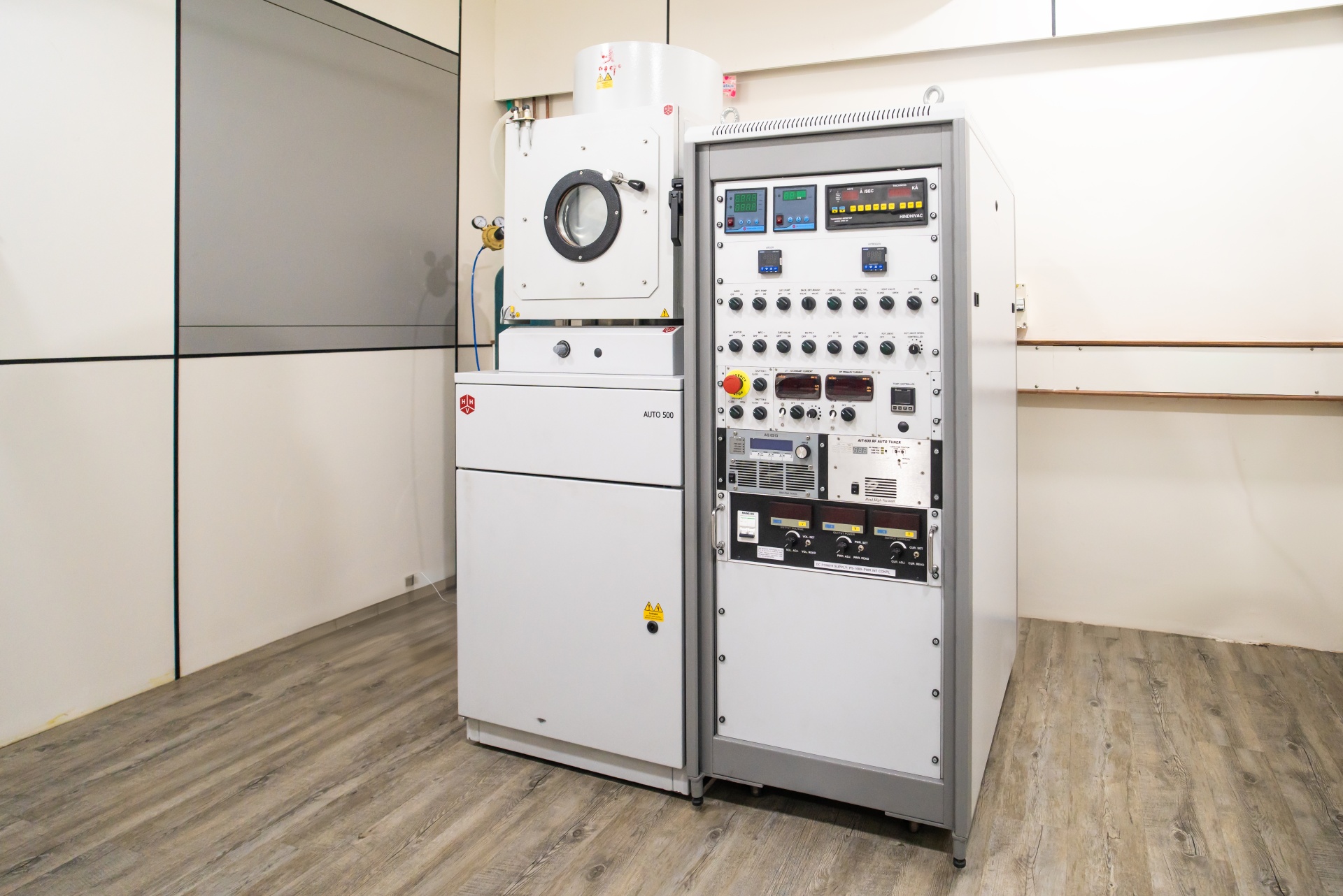
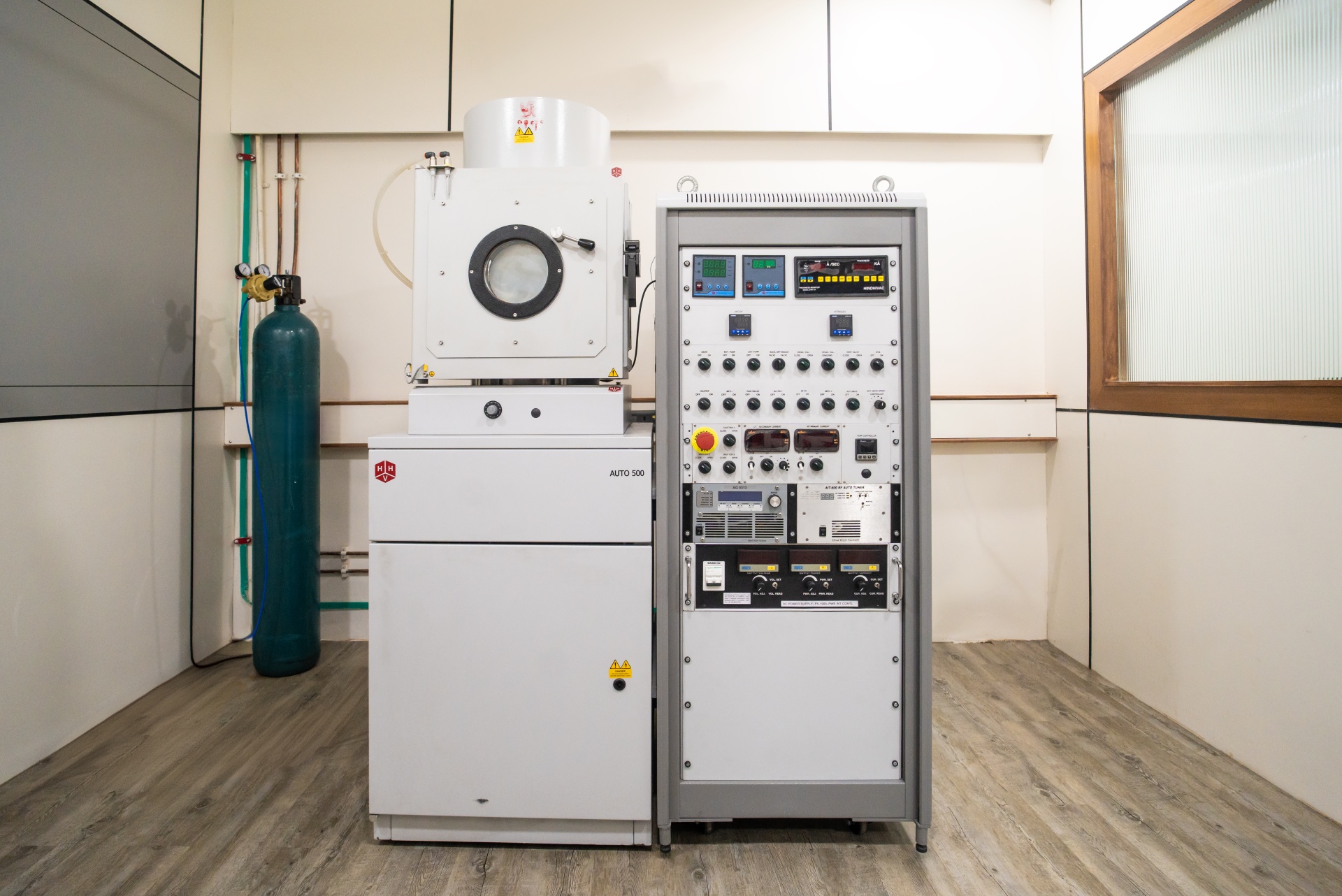
The Auto 500 - Three Methods in One Chamber
What distinguishes the Auto 500 from simpler deposition systems is its three-in-one capability. Most research laboratories require separate instruments for conducting and non-conducting material deposition. The Auto 500 integrates all three primary deposition techniques in a single vacuum chamber, enabling complete multilayer device structures to be built without ever breaking the vacuum – and therefore without any atmospheric contamination between layers.
DC Magnetron Sputtering - For Conductive Materials
DC sputtering uses a constant high-voltage electric field to ionise argon gas into a plasma. Positively charged argon ions are accelerated toward the negatively charged target material, colliding with it at high velocity and knocking off atoms through a process called physical sputtering. These ejected atoms travel through the vacuum chamber and deposit on the substrate, forming the thin film. A bank of permanent magnets behind the target (the “magnetron”) confines electrons near the target surface, dramatically increasing the ionisation rate and enabling denser, better-adhering films at lower chamber pressures. The MNRDC’s DC power supply (1 kW by HHV) provides high-power sustained bombardment for metals like titanium, molybdenum, chromium, and copper.
RF Magnetron Sputtering - For Insulators and Oxides
RF sputtering solves a specific problem: when a DC electric field is applied to a non-conductive target material such as silicon dioxide or titanium dioxide, electrical charge accumulates on the target surface and stops the sputtering process. By applying a radio frequency (RF) signal at 13.56 MHz – the internationally standardised frequency for industrial/scientific RF equipment – the field alternates fast enough to prevent charge accumulation while maintaining the plasma. This enables deposition of any material, conductive or not. The MNRDC’s RF power supply (300W, 13.56 MHz by Barthel/T&C) includes auto-tune matching to minimise reflected power and ensure stable plasma operation.
Thermal Evaporation - For Soft Metals and Organics
Thermal evaporation is the simplest of the three methods: a resistive heating element (boat or filament) holds the source material. When current passes through the element, it heats the source material to its evaporation temperature, and the vapour rises and condenses on the substrate above. This method is gentle and produces very smooth, low-stress films – ideal for gold, silver, and organic semiconductor layers where the high-energy ion bombardment of sputtering could damage the material. Deposition Thickness Measurement Devices (DTMs) are used exclusively with thermal evaporation to monitor film growth rate in real time.
Key Technical Parameters at the MNRDC
The Auto 500 vacuum chamber is a 500mm × 500mm × 500mm stainless steel enclosure with front-loading access. The vacuum system uses a rotary pump for initial roughing (reducing pressure from atmospheric to ~10^-2 Torr) followed by a turbomolecular pump for high-vacuum conditions (achieving ~10^-6 Torr) – eliminating virtually all air molecules from the deposition path. Chamber pump-down takes approximately 15 minutes to reach the deposition-ready vacuum.
The substrate holder accommodates wafers up to 100mm diameter, rotates at up to 20 RPM to ensure uniform film thickness across the entire substrate, and heats to 600°C with PID temperature control via a K-type thermocouple. Higher substrate temperatures produce denser, better-crystallised films because arriving atoms have more energy to find stable surface sites. The target-to-substrate distance is 8-10cm, measured from the cap to the insulating layer.
Gas flow is controlled by dedicated Mass Flow Controllers (MFCs) for argon and nitrogen, enabling precise control of the deposition atmosphere. Reactive sputtering – where nitrogen or oxygen is added to react with the sputtered metal atoms and form nitride or oxide films – produces materials like titanium nitride (TiN), silicon nitride (Si3N4), and titanium dioxide (TiO2) in a single step.
What the MNRDC Can Deposit - Applications
Metal films for contacts and reflective layers include aluminium, titanium, chromium, molybdenum, gold, silver, and copper. Oxide films for insulating and optical layers include silicon dioxide, aluminium oxide, indium tin oxide (transparent conductor), zinc oxide, and titanium dioxide. Nitride films for hard coatings include titanium nitride (one of the hardest thin film materials available – used on cutting tools and medical implants) and silicon nitride. Complete multilayer structures for solar cells, sensors, and photonic devices can be built in a single session.
A practical example from the MNRDC: fabricating a solar cell test structure begins with DC sputtering of a molybdenum (Mo) back contact on glass, followed by RF sputtering of a nitride buffer layer, followed by RF sputtering of an ITO transparent front electrode – all deposited sequentially in the same chamber without vacuum break. This workflow, impossible without the Auto 500’s three-method architecture, produces clean, well-defined multilayer devices directly comparable to those produced in semiconductor fabrication facilities. For further context on thin film solar cell research, the MNRDC’s own green hydrogen publication in Renewable Energy demonstrates the center’s broader thin film research capabilities.
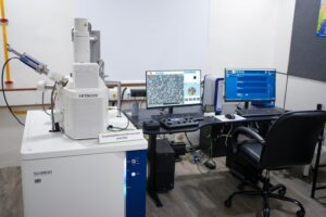
Students in B.Tech Chemical Engineering, B.Tech Electronics and Communication Engineering, and B.Sc Physics at Parul University can access the sputtering system for research projects under MNRDC supervision. The combination of thin film deposition and the center’s SEM, XRD, and AFM characterisation creates a complete thin film research workflow in one facility.
FAQs
What is the difference between DC sputtering, RF sputtering, and thermal evaporation?
DC sputtering uses a constant high-voltage field and is used for conductive target materials (metals). RF sputtering uses a 13.56 MHz alternating signal to prevent charge accumulation and is used for non-conductive materials (oxides, nitrides). Thermal evaporation heats the source material until it evaporates and is used for soft metals (gold, silver) and organics. The MNRDC's Auto 500 combines all three in one chamber.
What thin films can the MNRDC deposit by sputtering?
The MNRDC can deposit metals (Ti, Mo, Cr, Al, Au, Ag, Cu), oxides (SiO2, Al2O3, ITO, ZnO, TiO2), nitrides (TiN, Si3N4), and complete multilayer device structures for solar cells, sensors, and photonic devices. Reactive sputtering in the nitrogen or oxygen atmosphere produces nitride and oxide films from metal targets in a single deposition step.
What is the maximum substrate temperature during deposition at the MNRDC?
The substrate heater in the Auto 500 supports temperatures from room temperature to 600°C, with PID temperature control via a K-type thermocouple for accurate and stable heating. Higher substrate temperatures produce denser, better-crystallised films because arriving atoms have more energy to migrate to stable lattice sites - important for epitaxial films and highly crystalline coatings.
How does magnetron sputtering differ from basic sputtering?
In magnetron sputtering, permanent magnets behind the target create a magnetic field that traps electrons near the target surface. This dramatically increases the probability of electron-argon collisions and the resulting argon ionisation rate - creating a much denser plasma near the target. The result is higher deposition rates, more stable plasma operation at lower pressures, and better-quality films compared to basic (non-magnetron) sputtering.