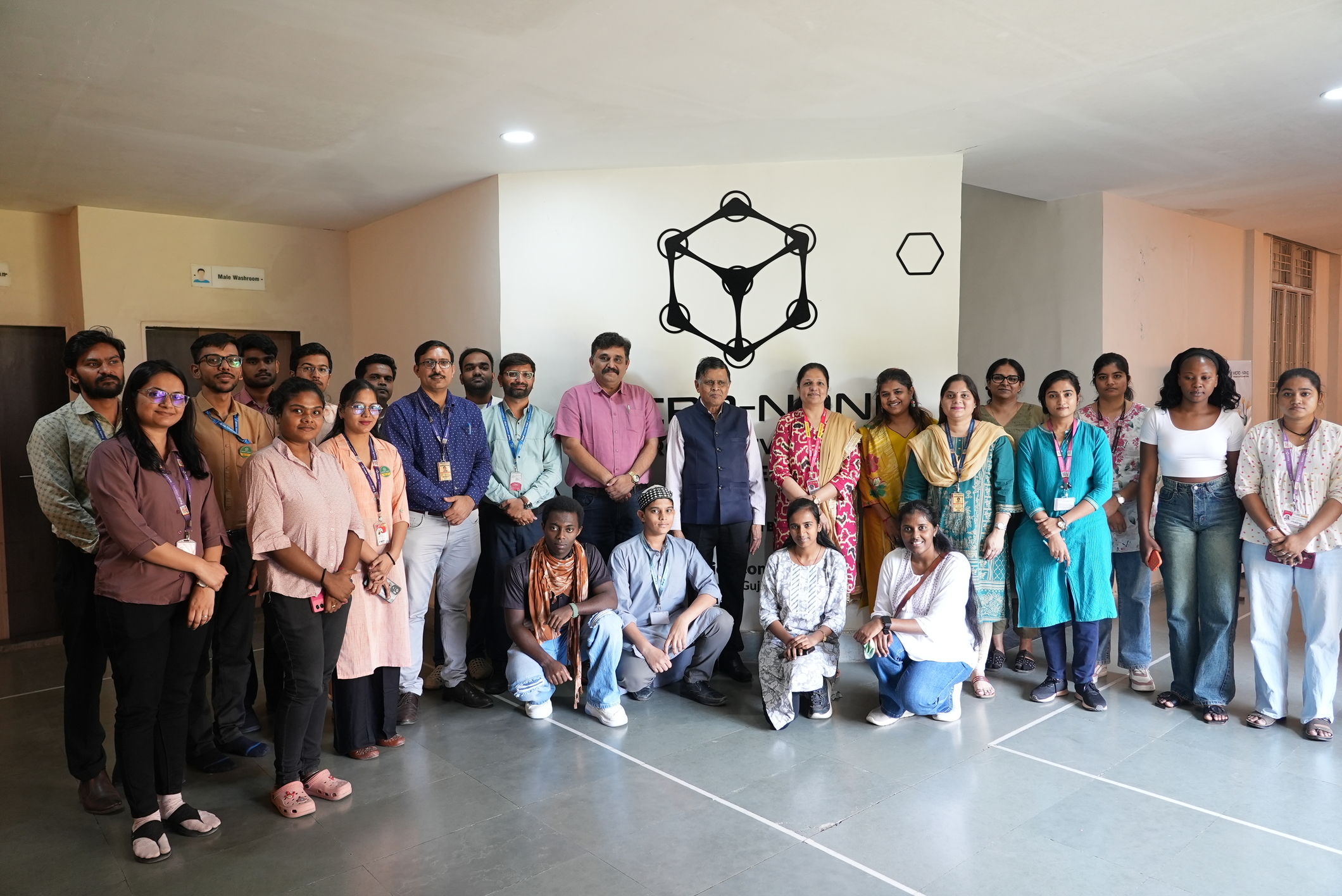
Before the science and there’s plenty of science coming the speaker deserves proper context. Because who’s delivering a lecture shapes how every word lands. And in this case, someone who does Indian materials research doesn’t produce very often.
Prof. Dr. V. Ganesan Former Centre Director of the UGC-DAE Consortium for Scientific Research in Indore. For anyone outside Indian academia, here’s what that means in plain language: the UGC-DAE Consortium is one of the backbone organisations that keeps university-level physics research functional across this country. It’s infrastructure. It’s an instrument. It’s the machinery everyone else depends on. Running it isn’t a reward for publishing well. It’s a trust the national scientific establishment places in someone they believe can keep the whole engine turning. He’s currently Dean of Research Affairs at Medical University, Indore.
- Approximately 500 research papers published.
- Over 10,000 citations.
- CSR Scientific Excellence Award holder since 2010.
- President of the Indian Physics Association’s Indore Chapter.
Four decades into a career studying how matter behaves at the atomic scale, and the wonder hasn’t cooled even slightly. That tells you something about the field. He spoke about;
- His research domains, listed here for breadth, not for memorisation: Low-Temperature Physics and Cryogenics.
- Scanning Probe Microscopy. Physics of superconductivity and magnetism. Rare-earth and actinide compounds. Advanced thermoelectric materials and devices.
- Magnetic and transport properties of perovskites. Zinc oxide doping and properties. Woven through all of it like a spine holding the skeleton together sits his expertise in Atomic Force Microscopy and X-ray Photoelectron Spectroscopy. AFM isn’t one instrument among many in his toolkit. It’s the lens he picks up first. It’s the one he’s been reading materials through for 40 years straight.
Science as Imagination - Setting the Stage
No formula on the first slide. No diagram. No Greek alphabet crowding the screen. Prof. Ganesan opened with a question.
What makes scientific discovery possible?
Not equipment. Not funding. Not your h-index or how many DST grants you’ve bagged or which journal responds to your emails. Imagination. That was his answer. A man with 500 published papers looked at a room full of researchers and said the single most important ingredient is the one no vendor catalogue sells.
He brought in Nobel Prize-winning discoveries in X-ray physics cases where someone made a conceptual leap the data alone wouldn’t have suggested, saw something nobody else was looking for, and cracked open an entire field. His point was direct.
Build the most expensive lab in India. Import the shiniest instruments. Staff it with the sharpest postdocs from the best programmes. If nobody in that lab can imagine what a result might look like before the machine confirms it, discoveries will sit right there in the data. Undiscovered. Because nobody imagined them first.
Then came Ramanujan. Srinivasa Ramanujan. And Shakuntala Devi. Not physicists. Not materials scientists. In a materials science workshop. But that was precisely the point. Ramanujan didn’t arrive at his results through proper channels. Nobody taught him the formal route. His mind simply went there.
Shakuntala Devi processed numbers in ways that no formal training could explain or replicate. Prof. Ganesan connected that kind of thinking sideways, unconventional, arriving from angles nobody else considers straight to the nanoscale.
Science as imagination and communication. That framing imagination plus communication set a tone that no other session across the three-day workshop came close to matching. If you wish to amp your career in Micro Nano Research & Development center, enrol into Bachelor of Science in Biotechnology now!
And for researchers, the ones grinding through, you can explore Master of Science in Biotechnology and create a Sustainable and Healthier Future ahead. Permission to believe the love for the work doesn’t have to die somewhere around your second postdoc. Prof. Ganesan, standing there at the front of that boardroom, was living proof it doesn’t.
Surface Characterisation - Why the Surface Changes Everything
Science time. And the goal here is to explain this the way Prof. Ganesan did cleanly, honestly, without pretending it’s simpler than it is, and without assuming everyone reading this has already cleared NET. Some readers are deep into materials research. Some might be second-year BSc students trying to figure out what surface characterisation even means.
Why would someone spend an entire career on just the surface? Why not study the whole material? Here’s the answer, and once this clicks, everything in the rest of the article makes sense.
Pick up a bulk material. A steel I-beam at a Vadodara construction site. A copper wire running through a wall. A slab of Makrana marble. The surface exists, obviously, but it’s a laughably tiny fraction of the total volume. Bulk properties dominate. The inside runs the show. Surface matters, sure, but not that much.
Now shrink that material. Micro scale. Shrink further. Nano scale. Watch the ratio between surface area and volume. It explodes. At the nanoscale, the surface isn’t a thin coat of paint on a big wall anymore. The surface is most of the material. There’s barely any bulk left. Almost all surfaces. And any change at the atomic level one misplaced atom, a tiny chemical contamination, a defect one nanometre across, directly affects how the entire material performs. Not indirectly. Not through a chain of events.
A material’s surface determines how it talks to its environment. How it bonds to other materials. Whether it conducts electricity or refuses to. How it responds to heat, pressure, chemical attack, biological fluids. Get the surface wrong and the nanomaterial is useless. It doesn’t matter how perfect the crystal structure is three layers down. The surface is where the conversation between the material and the world happens. Everything else is backstage.
Prof. Ganesan made this point early in the session. Made it again from a different angle. Made it a third time for anyone still catching up. Because this surface-dominance idea is the entire reason every instrument he was about to discuss exists. SPM. STM. AFM. MFM. Every acronym that followed was invented to answer one question: what is happening on that surface, and how do we measure it with enough precision to actually learn something we can use? So, if you’re passionate about building a career in nanotechnology, book your slot for a Bachelor of Science in Biotechnology today!
Signal vs Noise - The Precision Imperative at Nanoscale
Before getting into individual instruments, Prof. Ganesan paused. Set the acronyms aside. And delivered what might have been the most practically valuable five minutes of the entire three-day workshop.
Signal versus noise.
Sounds elementary. Signal is the actual data of what the surface is doing. Noise is everything else. Simple? At the human scale, yes. At the nanoscale? It’s a nightmare.
At nano, the signal from the surface is tiny. And the noise is the entire physical universe conspiring against the measurement. The HVAC system humming through the building’s walls? The AFM picks that up. A truck on the road outside? That vibration travels through the ground, up the foundation, through the floor, into the instrument table, into the cantilever, and appears in the data as a bump that looks exactly like a real surface feature.
Prof. Ganesan was absolutely serious about this. Vibration isolation systems, he said, are prerequisites. He stressed the word. Prerequisites. Not Phase 2. Not “after the next grant cycle.” Not a line item that can be pushed to next year’s budget. Prerequisites. Without proper vibration isolation, a lab isn’t doing nanoscale research. It’s recording the building’s heartbeat and calling it science. And this is the terrifying part nobody will know. The noise looks like a signal. Papers get published.
Prof. Ganesan, in roughly four minutes, moved it to the top of their list. Possibly saved some PhD students years of unusable work. That’s the kind of wisdom that comes from 40 years of actually running instruments, not reading about running them, not supervising someone else who runs them, but running them personally. The textbooks don’t include this lesson. Most textbook authors haven’t spent enough hours in the lab to know what goes wrong when the building vibrates.
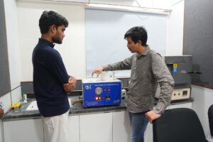
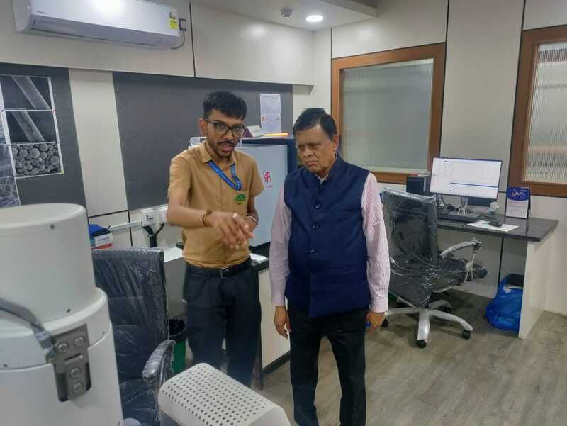
Atomic Force Microscopy - From Theory to Research Practice
Atomic Force Microscopy, born in 1986 because STM was breathtaking but also for most materials science maddeningly useless. It only worked on conductors, and the world is overwhelmingly made of things that don’t conduct. The conceptual fix was gorgeous in its simplicity. Don’t measure current, measure force.
Prof. Ganesan walked through the mechanics with the care of someone who’s explained this countless times and still thinks it deserves careful explanation every time. Here’s the setup. A sharp tip similar concept to STM mounted on a cantilever. A tiny, flexible beam. Picture a diving board at the university swimming pool. Except this diving board is maybe 100 micrometres long and has a needle at its end that’s a few nanometres wide at the tip.
As this tip scans across a surface, forces between tip and surface van der Waals forces, electrostatic interactions, all those atomic-scale pushes and pulls cause the cantilever to deflect. A laser beam bounces off the cantilever’s back surface onto a position-sensitive photodetector. The detector registers every tiny deflection with precision that borders on unreasonable. Ready to specialise in nanotechnology? Start your journey with a Master’s in Biotechnology.
Magnetic Force Microscopy and Cowburn Analysis
- Same skeleton as AFM. Same cantilever. Same laser detection. One crucial difference is that the tip gets coated with magnetic material. And that one change opens up a completely different dimension of information. As the magnetically coated tip scans across a surface, it doesn’t just feel physical forces anymore.
- It feels magnetic forces. It maps the magnetic domain structure of materials, the invisible geography inside a magnetic material where magnetisation points this direction in one region and that direction in the next, separated by domain walls too small and too subtle for any optical method to see but absolutely critical to how the material behaves magnetically.
- Prof. Ganesan illustrated this with cobalt thin film examples. The kind of films used in magnetic storage research. Hard drives. The devices holding every photo, every email, every document, every piece of digital life that matters to anyone reading this. Understanding the magnetic domain structure of those films isn’t an academic exercise. It’s the difference between a drive that stores data reliably and one that corrupts it. Between a device you trust and one that betrays you.
- He then moved into Cowburn analysis – R. P. Cowburn’s studies of magnetic nanostructures. If that name doesn’t ring a bell for non-specialists, it should, because Cowburn’s work reshaped understanding of how magnetism organises itself at the nanoscale. Prof. Ganesan covered domain structures, magnetisation behaviour, switching mechanisms, what happens when a magnetic domain flips from one state to another, the physics of that tiny event that makes digital memory possible and spin-dependent transport.
- The applications? MRAM aka magnetoresistive random access memory, the technology fighting to become the next generation of computer memory. Hard disk technology. Nanomagnetic devices. Anywhere the question is “what are the magnetic domains doing at scales too small for any other technique?” MFM provides the answer and Cowburn’s framework helps interpret it.
FAQs
What is surface characterisation and why does it matter in nanotechnology?
Surface characterisation is the study of physical, chemical, mechanical, and electronic properties of a material’s outermost layers, the skin, essentially. At the nanoscale, it becomes critical because the surface-to-volume ratio shoots up enormously. The surface isn’t a wrapper anymore it is most of the material. Which means atomic-level changes on the surface directly control everything that matters: electrical conductivity, mechanical strength, chemical reactivity, biological compatibility. Understand the surface and you understand the material. That’s why entire careers and entire laboratories Prof. Ganesan’s 40-year career among them is devoted to it.
What is the difference between STM and AFM?
STM - Scanning Tunneling Microscopy relies on quantum mechanical electron tunneling between a conducting tip and a conducting sample. Keyword: conducting. Both must carry electricity. Beautiful atomic resolution on metals but completely useless for insulators, polymers, biological samples, ceramics. STM’s conductivity requirement locked out 80-90% of the materials scientists actually wanted to study. That invention blew the field wide open.
What is Magnetic Force Microscopy used for?
MFM takes a standard AFM setup and adds a magnetically coated tip. Instead of feeling only physical forces, the tip now senses magnetic forces, mapping the domain structure of magnetic materials at the nanoscale. Where is the magnetisation pointing? Where are the domain walls? How do they behave under applied fields? This matters for magnetic storage media, spintronics, MRAM, magnetoresistive random access memory, the next generation of computer memory and condensed matter physics broadly.
Who is Prof. Dr. V. Ganesan?
Former Centre Director of the UGC-DAE Consortium for Scientific Research, Indore. Currently Dean of Research Affairs at Medicaps University. Nearly 40 years of research experience. 500-plus publications. 10,000-plus citations. CSR Scientific Excellence Award 2010. President of the IPA-Indore Chapter. One of India’s foremost experts in Scanning Probe Microscopy, Low-Temperature Physics, and advanced condensed matter physics. And based on every single participant's response from this workshop, one of the most engaging scientific communicators working in the country today.