When working with advanced materials, one common question arises: Which characterisation technique should I choose: XRD, SEM, or AFM? Each method provides different information about a material. Selecting the correct test depends on whether you want to study surface features, internal crystal structure, or nanoscale roughness.
At the MicroNano Research & Development Centre MNRDC, these three advanced techniques are available under one roof, allowing comprehensive micro to nano scale analysis. Understanding their differences will help you choose the right tool for your research sample.
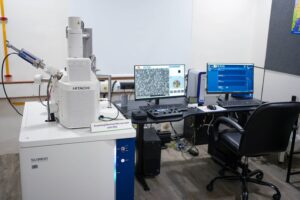
1. SEM (Scanning Electron Microscopy)- For Surface Morphology
What SEM Does
SEM is primarily used to analyse surface structure and morphology. It generates high resolution grayscale images showing:
- Particle size and distribution
- Surface texture
- Micro cracks and defects
- Coating thickness
- Wear tracks
The system operates using an electron beam generated by a tungsten filament and focused onto the sample. Images are typically captured at resolutions such as 30 µm, 10 µm, and 5 µm.
When to Choose SEM
Choose SEM if you want to:
- Visually inspect surface defects
- Study fracture surfaces
- Examine nanoparticles
- Analyse coating morphology
- Observe corrosion or wear damage
SEM is used to analyse surface morphology and is the appropriate technique for studying surface appearance, cracks, and particle distribution.
Added Advantage: SEM + EDS
SEM can be combined with EDS to verify elemental composition and material purity. This is helpful when confirming alloy composition or identifying contaminants.
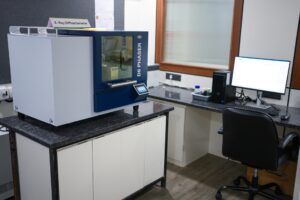
2. XRD (X-Ray Diffraction) – For Internal Structure & Phase Identification
What XRD Does
While SEM looks at the surface, XRD examines the internal atomic arrangement: the material’s “skeleton”.
XRD determines:
- Crystal structure
- Phase composition
- Residual stress
- Crystallite size
- Lattice parameters
It works based on Bragg’s Law nλ = 2d sinθ, which relates X ray wavelength, atomic spacing, and diffraction angle.
The output is an Intensity vs 2θ graph, where sharp peaks act as a fingerprint of the material.
When to Choose XRD
Choose XRD if you want to:
- Identify unknown materials
- Confirm phase changes after heat treatment
- Measure crystallinity
- Analyse thin films using GIXRD
- Determine coating thickness and roughness using XRR
XRD is used to determine internal crystal structure, phase composition, and atomic arrangement, making it the appropriate technique for identifying what a material is made of internally.
Special Strength
XRD is a Non Destructive Testing NDT technique, meaning the sample remains unharmed after testing.
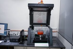
AFM (Atomic Force Microscopy) – For Nanoscale Surface Measurement
What AFM Does
AFM provides nanoscale surface mapping by physically “feeling” the surface with an ultra sharp tip 510 nm radius.
It measures:
- Surface roughness
- Step height
- Grain size
- Nano mechanical properties
AFM operates using Hooke’s Law F = kx, measuring cantilever deflection as the tip scans the surface.
It produces:
- 2D topography maps
- 3D surface models
- Roughness reports with ISO standard parameters
Imaging Modes
AFM offers multiple modes:
- Contact Mode direct dragging
- Non Contact Mode hovering
- Tapping Mode vibrating tip; most commonly used
When to Choose AFM
Choose AFM if you want to:
- Measure nanoscale roughness
- Study thin film surface uniformity
- Analyse optical coatings
- Evaluate grain distribution
- Examine delicate biological samples
AFM measures nanoscale surface roughness, height variations, and topographical features, making it the ideal technique for evaluating surface smoothness at the nanometer level.
Quick Comparison Table
| Feature | SEM | XRD | AFM |
| Main Focus | Surface morphology | Internal crystal structure | Nanoscale surface topography |
| Output Type | Grayscale images | Diffraction peaks graph | 2D/3D maps + roughness values |
| Measures Composition? | Yes with EDS | Yes phase identification | No |
| Measures Roughness? | Limited | No | Yes |
| Non Destructive? | Yes | Yes | Yes |
How to Decide Based on Your Research Goal
Scenario 1: You developed a new alloy and want to confirm its phases.
Choose XRD.
Scenario 2: You want to check if a coating has cracks or defects.
Choose SEM.
Scenario 3: You need to measure whether a lens surface roughness is below 100 nm.
Choose AFM.
Scenario 4: You want both structure and composition.
Use SEM + EDS, possibly combined with XRD.
Can They Be Used Together?
Yes, and often they should be.
For example:
- Use XRD to confirm phase composition.
- Use SEM to inspect microstructure.
- Use AFM to measure nanoscale roughness.
Each method answers a different scientific question. Together, they provide complete material characterisation.
Final Thoughts
There is no single “best” test. The right choice depends entirely on your research objective.
- Choose SEM for surface imaging.
- Choose XRD for crystal structure and phase analysis.
- Choose AFM for nanoscale roughness and precision surface mapping.
Understanding the strengths of each technique ensures accurate data, efficient testing, and meaningful scientific conclusions. When selected correctly, these tools transform a simple material sample into a fully understood scientific system.