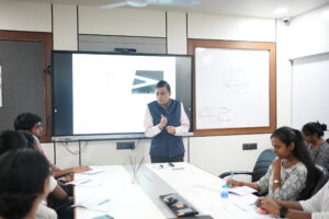

His one-hour lecture for an interdisciplinary audience covering pharmacy, civil engineering, biotechnology, Ayurveda, and genetics systematically addressed SEM components, imaging modes, critical operating parameters, AFM measurements, and quantitative image analysis. Multiple participants called it the session they most needed.
Here’s something that doesn’t happen often enough in Indian research universities. A scientist who’s genuinely good at operating complex instruments and genuinely good at teaching non-specialists how to make sense of the data those instruments produce. Those are two completely different skills. Most people have one or the other. Dr. Mahendra Singh Rathore happens to have both. He serves as Associate Professor (Research Cadre) in the Department of Applied Sciences and Humanities at Parul University, and MNRDC. That word embedded matters. He’s not a visiting faculty member who flies in, delivers a guest lecture, and disappears. He sits inside the research center.
His role combines active research with training researchers from across disciplines, which makes him uniquely positioned to take complex instrumentation knowledge, the kind that usually lives in the heads of three or four people in a country and translate it for audiences who need the data but didn’t train as physicists.
Pharmacy people. Civil engineers. Biotech scholars. Ayurveda researchers. All of them sitting in the same room, all of them generating SEM and AFM data they can’t fully read. That’s the gap Dr. Rathore fills.
He’s also a core member of the MNRDC. Not just someone who uses the instruments. Someone who shapes how the center plans its research, prioritises its training, and builds bridges to disciplines that would otherwise never walk through the MNRDC’s doors.
Defining Surface Analysis
Let’s get the definition right first, because getting this wrong trips up everything that follows. Dr. Rathore defined surface analysis precisely: the study of the chemical structure, morphology, roughness, defects, and texture of the outermost atomic layers of a solid material. Not the inside. Not the bulk. The outermost layers. The part of the material that’s actually doing the talking when it interacts with the world.
And then he flagged something that honestly a surprising number of researchers overlook. Surface properties are frequently different from bulk properties. Different. Not “slightly varied.” Different. A material’s real-world behaviour isn’t governed by what’s happening three layers deep. It’s governed by its outermost layers.
The chemistry on the surface, the roughness on the surface, the defects on the surface determine whether a drug delivery particle works or fails, whether a coating sticks or peels, whether a catalyst performs or sits there doing nothing. The bulk can be textbook-perfect and the surface can still betray you.
He introduced four broad categories of surface imaging techniques.
- Electron-based: SEM, TEM.
- Probe-based: STM, AFM.
- Ion-based.
- Optical.
Four families. Each with its own physics. Each suited to different materials and different questions. Technique selection, he stressed, depends on two things: what material you’re looking at and what information you need from it. There’s no universal tool. There’s only the right tool for the right question.
SEM - Historical Development
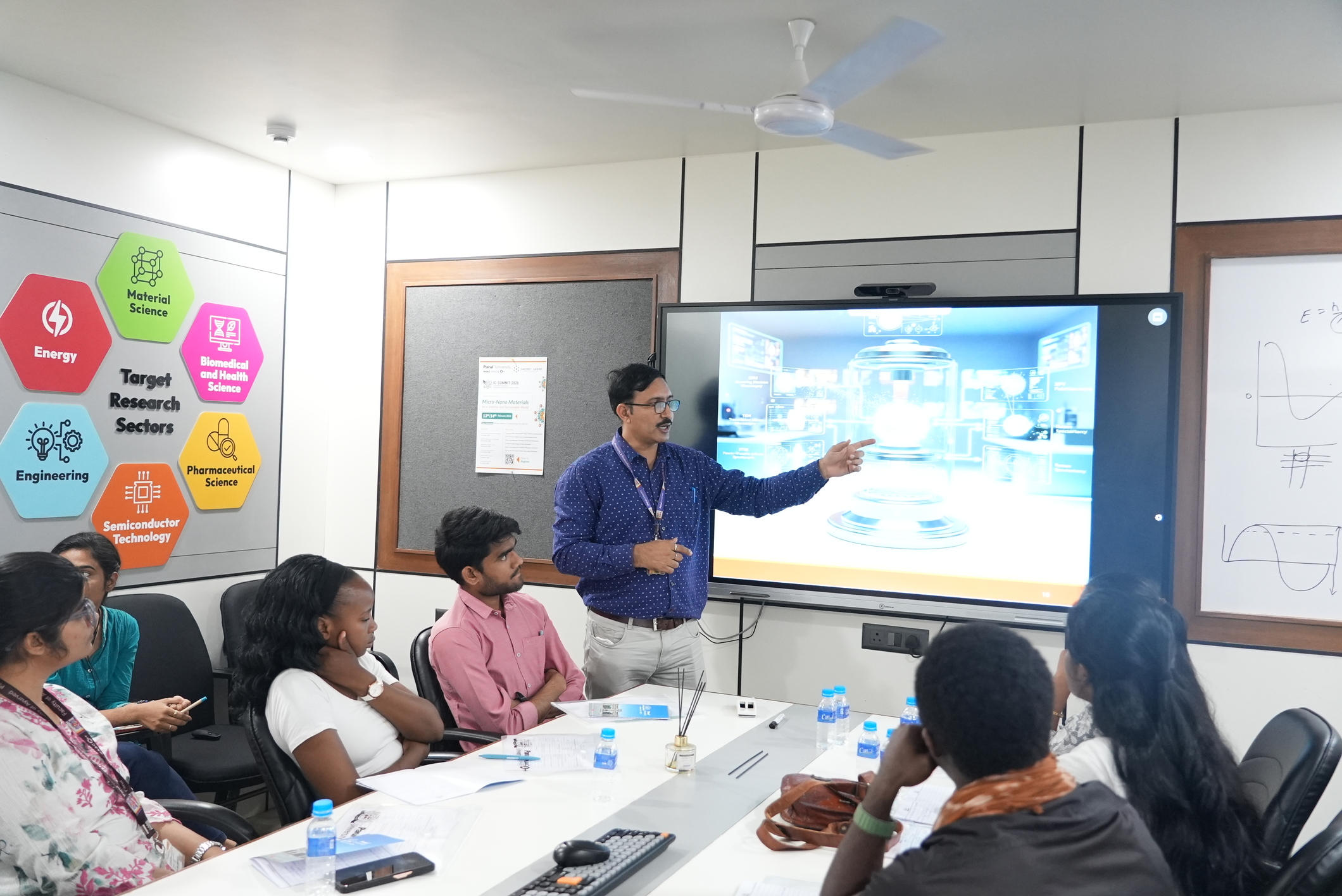
Before diving into how SEM works now, Dr. Rathore took the room backward. History. Because understanding where an instrument came from, what problem it was built to solve, what limits it was designed to break changes how you think about using it.
The story starts with frustration. Visible-light microscopy had a ceiling. Resolution limited by the wavelength of light. Below a certain size, you simply couldn’t see any finer detail. The image blurred. Physics said no. So scientists asked a different question: what if we used electrons instead of photons? Electrons have much shorter wavelengths. Which means much higher resolution. The “electron microscope” was born from that question.
Dr. Rathore traced the development through the people who built it. Max Knoll. Manfred von Ardenne. Ernst Ruska, the man awarded the Nobel Prize in Physics in 1986, credited as the father of electron microscopy for the instrument he built in 1932. This principle is almost a century old. But the instrument has evolved beyond recognition from those early, room-sized, temperamental machines to the modern arsenal: high-resolution SEM, low-voltage SEM, in-situ SEM, analytical SEM.
Dr. Rathore showed this evolution on screen. Early instruments next to modern ones. The contrast was stark. And the point was clear before learning what buttons to press, understand the shoulders you’re standing on. Know who struggled with resolution limits in 1932 so that you could imagine nanoparticles in 2026. That context isn’t decoration. It’s respect. And it shapes how seriously you take the instrument when you sit down in front of it.
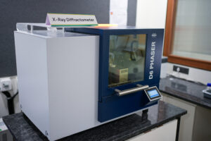
Key SEM Components - Systematic Walkthrough
This was the section where Dr. Rathore’s teaching instinct really showed. He didn’t just list components. He displayed photographs of each one as he introduced it. Actual photos. Not diagrams from a textbook. Photos of the physical parts inside a real SEM. For researchers who’d been sending samples to a testing lab and receiving images back without ever seeing the inside of the machine, this was the first time many of them understood what’s actually in there.
- The Electron Gun – Sits at the top of the column. Generates the primary electron beam. Two main types of tungsten filament, which is the workhorse, the affordable one, the one most university labs run and Field Emission Gun – Produces a brighter, more coherent beam but costs significantly more. Choice between them depends on budget and resolution requirements.
- Magnetic Lenses & Condenser lens and objective lens – These focus the beam electromagnetically, not optically. And here Dr. Rathore made a point that seems obvious once you hear it but that some participants hadn’t considered: glass cannot focus electrons. Electrons aren’t photons. You can’t use optical lenses. You need magnetic fields to bend the electron path. Completely different physics from the microscope in a school biology lab.
- Scanning Coils – These raster the beam across the sample surface — moving it back and forth, line by line, like reading a page. Every point on the surface gets hit by the beam. Every point generates a signal. The coils control where the beam goes.
- The Sample Chamber and Stage – Where the sample lives during imaging. Vacuum-sealed because electrons scatter off air molecules, so the beam needs a clear path. The stage provides X, Y, Z movement plus tilt and rotation. Need to look at the sample from a different angle? Tilt the stage. Need to zoom in on a different area? Move X and Y. Need to focus? Adjust Z. Simple controls, but understanding what each one does prevents the kind of confused button-pressing that wastes beam time.
- Two detectors. The SE Detector collects secondary electrons, low-energy electrons knocked off the surface by the beam. These give you surface topography. The shape of the surface. The hills and valleys. The BSE Detector collects backscattered electrons, high-energy primary electrons that bounce back from deeper within the sample. These give you compositional contrast. Different elements, different brightness. Heavier atoms scatter more electrons back. Heavier appears brighter.
Dr. Rathore went through each component slowly. Pointed at each photo. Explained what it does, why it’s there, and what happens when it malfunctions. For an audience that included people who’d never opened an SEM column, this was the walk-through that turned a black box into an understandable machine.
Participant Response
The proof of a session’s value isn’t in the applause. It’s what people do after they leave the room. Srishti Rawal, a PhD scholar in chemical sciences. Working on heterogeneous catalysts. She’d been struggling with SEM result interpretation, not because she lacked intelligence but because nobody had ever taught her how to read the images properly. If you too want to explore possibilities in Chemical Domain, enrol into Parul University’s Bachelor of Technology in Chemical Engineering!
That gap had been slowing her research down. She specifically thanked Dr. Rathore during the review session, not with the generic “it was very informative” that academics deploy out of politeness, but with the specific, pointed gratitude of someone whose bottleneck just got cleared.
The session gave her the analytical framework she’d been missing. For someone with a mid-PhD, that’s not a nice-to-have. That’s potentially months saved.
Another one was Neha Kulshreshtha, a young and passionate Chemical engineering student. She described the image analysis content as so valuable that she video-recorded the session. Because she wanted to go back to it. Replay it. Catch the details she might have missed in real time. When a participant records a session on their phone, that’s the most honest feedback a speaker can receive. It means the content was too important to risk forgetting.
For participants across disciplines B.Pharm (Bachelor of Pharmacy), B.Tech Civil Engineering, B.Tech Biotechnology Engineering, and BAMS (Bachelor of Ayurvedic Medicine & Surgery) who had been receiving SEM and AFM test results from labs and struggling quietly with interpretation, Dr. Rathore’s session provided the missing piece.Not more data. Not better instruments. The ability to understand what the data they already had was actually saying. That’s the difference between having information and having knowledge. The information was always there. The knowledge arrived on February 25, 2026, in an MNRDC boardroom at Parul University. Inspired already? Join the movement, explore our Admissions for 2026 and begin your journey today.
FAQs
What is the difference between secondary electron and backscattered electron imaging in SEM?
Two detectors, two types of information. Secondary Electron imaging uses low-energy electrons knocked off the sample’s surface to escape from the top few nanometres, so SE images show surface morphology. Shape. Texture. Edges appear bright. The classic SEM “look.” Backscattered Electron imaging uses high-energy primary electrons that bounce back from deeper in the sample and here’s the key: BSE intensity scales with atomic number. Heavier elements scatter more. Heavier equals brighter. So BSE images reveal compositional differences. Two phases that look identical in SE can look completely different in BSE because their chemistry is different. SE tells you what it looks like. BSE tells you what it’s made of.
How do you choose the right accelerating voltage for SEM?
Depends entirely on the sample. The range is 1 kV to 30 kV. Higher voltages, tighter beam, better resolution, stronger signal. Great for metals, ceramics, and robust conductive materials. But high voltage on a fragile sample? Disaster. Polymers, biological specimens, non-conductive materials, they charge up, distort, and get physically damaged. For those, stay low. 1 to 5 kV. Accept slightly lower resolution in exchange for keeping the sample intact and the image clean. For EDS elemental analysis, higher voltages generate characteristic X-rays more efficiently so compositional work usually needs more kV than pure imaging. Every sample is a negotiation between resolution and preservation.
What surface roughness parameters can AFM measure?
The core set: Ra - arithmetic average roughness, the most commonly reported number. Rq - RMS roughness, more sensitive to extreme features than Ra. Rz - maximum peak-to-valley height. Areal equivalents Sa and Sq extend the measurement over a 2D area instead of a single line. Beyond these, height distribution histograms from AFM scans yield three powerful statistical descriptors meaning height, skewness. Together, these numbers describe surface homogeneity and character in language that’s quantitative, reproducible, and universally comparable.
Can SEM and AFM both be used on biological samples?
Both can. But the preparation requirements are worlds apart. SEM typically needs biological samples to be fixed, dried, and coated with a thin conductive layer, usually gold. That preparation kills and alters the sample. AFM doesn’t need any of that. It can image biological samples in liquid buffer solutions that mimic the body’s own conditions. Living cells. Hydrated proteins. How a cell’s mechanical properties change in response to a drug. That kind of data is invisible to SEM no matter how good the images look.