MNRDC, also known as the Micro Nano Research & Development Center at Parul University, functions the HHV Auto 500, which combines 3 deposition methods: DC magnetron sputtering, RF magnetron sputtering and thermal evaporation at low temperatures. This means a researcher can deposit a metal layer, then an insulating layer and then the organic layer, all in one run without ever opening the chamber to atmospheric contamination. The entire machine has executed 22 successful runs since the installation and is exclusively used for research ranging from solar cell fabrication to biomedical coating!
The Machine: HHV Auto 500 Specifications
- Model: Auto 500. Manufacturer: HHV Advance Technologies Pvt. Ltd. Cost: Rs 41,30,000
- Vacuum chamber: D-shaped, front-loading, stainless steel, approximately 500 mm x 500 mm x 500 mm
- Base pressure: approximately 10^-6 Torr (achieved via rotary pump + turbomolecular pump in sequence)
- DC power supply: 1 kW (HHV) for conductive targets (metals)
- RF power supply: 300W at 13.56 MHz (international standard) for non-conductive targets (oxides, nitrides)
- Substrate holder: up to 100 mm diameter, rotation to 20 RPM, heating from room temperature to 600C with PID control
- Gas lines: Argon (bombardment medium), Nitrogen (reactive sputtering for nitrides), Oxygen (reactive sputtering for oxides)
- Thermal evaporation: resistive heating boat/filament for low melting point materials
- Target-to-substrate distance: 8 to 10 cm
- Safety interlocks: cooling water flow, chamber pressure, door seal, power supply status
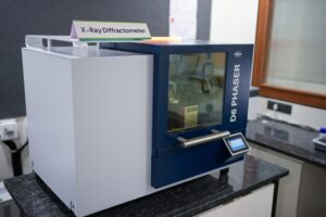
Uncover the Advanced XRD Capabilities & Possibilities at MNDRC, Parul University!
3 Prime Deposition Methods
DC Magnetron Sputtering: For Metals
Argon gas goes into the chamber and gets ionised into plasma. Now there are positively charged argon ions inside a vacuum, and they want to move toward something negative. The target material is that something – they hit it and knock atoms off the surface. Not melting, not cutting. Just knocking. Those atoms float across the chamber and land on the substrate sitting opposite. Hence, film builds up; that is the basic idea, and it is almost too simple until you realise how much can go wrong with it. The magnetron fixes most of what goes wrong. Permanent magnets behind the target pull electrons toward the surface and keep them there.
More electrons near the target means the argon ionises more aggressively in that zone. Denser plasma and faster deposition are executed as well. The whole thing runs more stable than it would without the magnets doing that work. Aluminium, titanium, chromium, molybdenum, gold, silver, copper, nickel, anything conductive works. That is the one condition.
RF Magnetron Sputtering: For Insulators
DC sputtering meets a non-conductive target and stops working. Charge builds up on the surface, has nowhere to go, and the plasma dies. Glass does this. Silicon dioxide does this. Any oxide does this.
The fix is not complicated once someone figures it out. Stop using direct current. Use a radio frequency signal instead, 13.56 MHz, oscillating fast enough that charge cannot accumulate before the field flips direction again. Plasma stays alive. Deposition continues.
Silicon dioxide, titanium dioxide, aluminium oxide, zinc oxide, indium tin oxide. All of these become depositable. None of them was possible with DC. One more thing worth mentioning: the RF supply runs an auto-tune matching network alongside it. Reflected power gets minimised. When reflected power is low, the plasma is stable, and the energy going in is actually reaching the target rather than bouncing back through the system.
Thermal Evaporation: For Soft Materials
Source material is placed into a resistive heating boat inside the chamber. Electric current heats the boat, melting and then evaporating the source material. The vapour rises and condenses on the substrate above, forming a smooth thin film. This method is gentler than sputtering and works best for materials with relatively low melting points: gold, silver, organic compounds for OLED devices, and sensor fabrication materials. Films produced by thermal evaporation tend to be very smooth with low internal stress.
Dielectric Testing at MNRDC Parul University
Why Vacuum, Rotation, and Heating Matter
- Vacuum: If air remained in the chamber, sputtered atoms would collide with air molecules and lose directionality before reaching the substrate. At 10^-6 Torr, atoms travel in straight lines from target to substrate. The mean free path (average distance before collision) becomes long enough for clean, efficient deposition.
- Rotation: Without rotation, the area directly above the target receives more material than the edges. The substrate rotates at up to 20 RPM, ensuring every part of the surface receives equal coating. This produces uniform film thickness from edge to edge.
- Heating: Cold substrates produce disordered, loosely packed films. When heated (up to 600C), arriving atoms have enough energy to find stable positions, producing denser, better-organised, more strongly bonded films. The PID controller maintains temperature within tight tolerances even as chamber conditions change during deposition.
What’s next after AFM Scan? BTS of the report outputs from MNRDC, Parul University!
Real Example: Building a Solar Cell Layer by Layer
The Auto 500 can fabricate a complete multi-layer solar cell test structure in a single session:
- Layer 1 (Back Contact): DC sputtering deposits molybdenum (Mo) onto a glass substrate
- Layer 2 (Buffer): Reactive RF sputtering in an argon/nitrogen atmosphere deposits a nitride buffer layer
- Layer 3 (Front Electrode): RF sputtering of an ITO target deposits a transparent conductive top layer
All three layers deposited in one continuous run. No vacuum break. No atmospheric contamination between layers. This is something that would require three separate machines and three separate loading sessions without the Auto 500.
Read more on – SEM testing at MNRDC
What Materials Can Be Deposited
- Metals: Aluminium, Titanium, Chromium, Molybdenum, Gold, Silver, Copper, Nickel
- Oxides: SiO2, Al2O3, ITO (Indium Tin Oxide), ZnO, TiO2 for insulating layers, optical coatings, transparent electrodes
- Nitrides: TiN (titanium nitride) and SiN for hard coatings and diffusion barriers
- Semiconductors: Silicon and Germanium for chip fabrication and photovoltaic research
- Organic and soft-metal films: via thermal evaporation for OLED devices and sensor fabrication
- Complete multilayer stacks: solar cells, sensors, photonic components, all without breaking vacuum
Applications
- Anti-reflective coatings: camera lenses, solar panels, eyewear
- Semiconductor manufacturing: metal and insulating layers inside microchips
- Solar cell research: conductive oxide, absorber, and buffer layers
- Hard coatings: TiN on tools and mechanical parts for wear resistance
- Biomedical devices: biocompatible coatings on implants, nanowire electrodes for nerve/heart cell signal detection
- Sensors: thin film sensing elements for pressure, gases, biological signals
- Data storage: magnetic films for hard drives and memory
- Scratch-resistant glass: protective layers on phone screens and optical surfaces
Read more on – AFM testing at MNRDC
Film Quality Assessment
After deposition, film quality is evaluated using MNRDC’s own characterisation instruments:
- Thickness: controlled by power, pressure, and time during deposition. Measured afterwards using XRD’s X-Ray Reflectivity (XRR) capability
- Surface roughness: measured by AFM at the nanoscale. A well-deposited film is mirror-flat at the atomic scale
- Crystal structure: determined by XRD. Temperature and power during deposition determine whether the film is crystalline or amorphous
- Adhesion: improved by substrate heating during deposition. Tested through standard adhesion methods
- Electrical properties: measured by the LCR Meter (ZM2376) for dielectric and impedance characterisation
This closed-loop, deposit on the Auto 500, characterise on SEM/XRD/AFM/LCR, all under one roof, is what makes MNRDC a complete thin film research facility rather than just a coating service.
Read more on – XRD testing at MNRDC
Preparation - How Cleanliness Determines the Holistic Film Quality
One fingerprint. That is genuinely all it takes. The film peels, cracks, grows unevenly, and the run is wasted. Contamination on the substrate surface does not show mercy based on how small it is, which is why the cleaning sequence before every run is fixed and non-negotiable.
- Distilled water first. Loose dust, surface particles, gone. Then acetone because water does not touch oils and greases and organic residues sitting on the surface. Acetone does. Then isopropyl alcohol or ethanol, specifically to chase out whatever acetone left behind. After all of that, the substrate dries completely before it goes anywhere near the chamber. Not mostly dry. Fully dry.
- Inside the chamber, aluminium foil lines the walls. When the run is done, the foil comes out, and fresh foil goes in. No scrubbing, no residue building up across sessions. Room temperature stays controlled throughout because unnecessary variables create unnecessary contamination, and there is no good reason to invite that. Gloves go on before any handling begins and stay on. None of this is overcaution. It is just what the process demands.
Read more on – Research at Parul University: Rs 25 Cr+ total funding
FAQs
How many methods of thin film coating are offered by MNRDC?
A total of 3 methods in one machine are run simultaneously in HHV Auto 500. DC magnetron sputtering, RF magnetron sputtering and thermal evaporation at low temperatures for soft materials & organics. Substrate heating at 600C, Argon, nitrogen and oxygen gas lines. Vacuum to 10-6 Torr, and 22 runs were completed.
Can MNRDC build multi-layer structures in one run?
Yes. The Auto 500 deposits multiple layers without breaking vacuum. Example: a solar cell with molybdenum back contact (DC sputtering), nitride buffer (reactive RF sputtering), and ITO transparent electrode (RF sputtering), all in one continuous session. No atmospheric contamination between layers.
How is film quality verified at MNRDC?
Using MNRDC's own instruments: XRD (crystal structure, XRR for thickness), AFM (nanoscale surface roughness), SEM+EDS (morphology and composition), LCR Meter (electrical properties). The complete pipeline from deposition to characterisation exists under one roof.