What Is Scanning Electron Microscopy and Why Does It Matter?
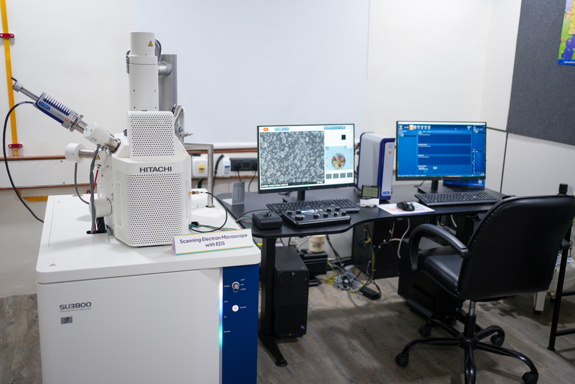
A Scanning Electron Microscope (SEM) is a scientific instrument that uses a focused beam of electrons instead of light to image the surface of a material. Because electrons have wavelengths far shorter than visible light, SEM can resolve surface features at scales that optical microscopy cannot reach down to approximately 3–4 nanometres in imaging resolution. The Hitachi SU3800 at the MNRDC achieves this standard resolution under optimal conditions.
The practical significance of this capability is enormous. A pharmaceutical company developing a drug formulation needs to know the size, shape, and distribution of drug particles to predict dissolution behaviour. A materials scientist developing a nanocomposite needs to verify that nanoparticles are dispersed uniformly rather than agglomerated. An aerospace engineer investigating a component failure needs to examine fracture surfaces at the microscopic level. A civil engineer characterising soil samples for a foundation project needs grain size and morphology data. All of these can be addressed with SEM.
The Hitachi SU3800 - Technical Specifications
The MNRDC’s SEM is the Hitachi SU3800 Hi-SEM, manufactured by Hitachi High-Tech India Pvt. Ltd. and installed in 2024 at a cost of ₹1.9 crore. It is paired with an EDS (Energy Dispersive Spectroscopy) unit and a sputter coater. The instrument has analysed over 897 samples since installation the highest utilisation rate of any instrument at the center, averaging 4–5 samples per day. The SEM accepts samples up to 100mm diameter × 50mm height.
How the SEM Works - From Electron Gun to Image
The SEM column begins with an electron gun at the top. The most common types used in research-grade SEMs are tungsten filament guns and Field Emission Guns (FEG). The Hitachi SU3800 uses a tungsten filament as its light source. High-speed electricity is applied to the filament, generating an electron beam that is directed downward by an anode and progressively focused by electromagnetic condenser and objective lenses glass cannot focus electrons, so magnetic fields are used instead.
Deflection coils raster the focused beam systematically across the sample surface line by line. As the primary beam interacts with the sample, it generates secondary electrons (SE) from near the surface and backscattered electrons (BSE) from deeper within the material. SE are collected by the SE detector for high-resolution surface topography imaging; BSE are collected by the BSE detector for compositional contrast imaging, where elements with higher atomic numbers appear brighter.
The entire process happens inside a sealed chamber maintained at high vacuum atmospheric molecules would scatter and absorb the electron beam, making imaging impossible. The vacuum pump-down process takes approximately five minutes from chamber sealing to beam activation.
SEM Imaging at the MNRDC - The Standard Workflow
Sample preparation is the first and most critical step. Solid samples are mounted on carbon tape on a 51mm or 125mm aluminium disc. Liquid samples are dried at 30–40°C under an incandescent bulb before mounting on copper tape. Non-conductive samples biological specimens, polymers, many oxides are sputter-coated with an ultra-thin layer of gold to prevent charge accumulation under the beam.
The prepared disc is mounted on the specimen stage, the chamber is sealed, and the vacuum pump-down sequence begins. Once the target vacuum is reached, an accelerating voltage is set: 5–30 kV for solid samples, 3–15 kV for liquid and semi-solid samples. The working distance is set to 5mm for standard SEM imaging.
Eight images are captured per sample, at magnifications progressing from low (30 µm scale) to high (5 µm scale), from different alignments and angles. Each image takes approximately 1 minute 10 seconds to capture. Scale bar, magnification, accelerating voltage, and working distance are automatically embedded in every image, ensuring complete traceability. Ready to grow in this domain? Join Parul University’s Master of Science in Biotechnology
EDS - Elemental Composition in the Same Session
The SEM is paired with an EDS unit, making it possible to determine the elemental composition of a sample in the same session as surface imaging without removing the sample from the chamber. EDS works by detecting the characteristic X-rays emitted by atoms when excited by the primary electron beam. Each element emits X-rays at specific energies, producing a spectrum that functions as an elemental fingerprint.
The MNRDC offers three EDS outputs: an elemental spectrum showing which elements are present and in what proportions; point analysis for elemental composition at a specific location; and area mapping, which colour-codes the spatial distribution of each element across the scanned region. The working distance for EDS is 10mm (compared to 5mm for imaging). A standard SEM + EDS session takes approximately 60 minutes, compared to 45 minutes for imaging alone.
Sample Types Analysed at the MNRDC
The range of samples the MNRDC’s SEM has analysed reflects the breadth of its user base. Pharmaceutical samples (drug particles, tablet surfaces, coating uniformity), ZnO and other oxide powders, titanium and silver metal specimens, plastic and polymer samples, battery electrode materials, ayurvedic oil residues (dried), human hair, teeth, and dog hair for biological and forensic characterisation, micro algae and biofilm specimens, and nanofibre samples all have been processed on the Hitachi SU3800.
The only categories of samples not accepted include those that are radioactive, explosive, highly corrosive, incompatible with high vacuum, or exceed the instrument’s size limits. Samples are occasionally rejected approximately once a fortnight typically for size non-compliance or contamination that would compromise the instrument or results.
Applications Across Research Fields
In materials science, SEM is used for grain size and grain boundary characterisation, phase distribution mapping, fracture surface analysis, and wear track examination. In pharmaceuticals, it enables drug particle size and shape analysis, tablet coating uniformity assessment, and nanoparticle characterisation for drug delivery systems. In nanotechnology, it visualises nanoparticles, nanorods, nanotubes, and nanowires. In biomedical research, it images tissues, cells, bacteria, and biofilms. In semiconductor and electronics research, it inspects lithography patterns and surface defects. In geology, it characterises mineral assemblages and pore structure in rock samples. In industrial quality control, it assesses surface finish and wear mechanisms.
Turnaround, Urgent Processing, and Output Delivery
Standard sample analysis at the MNRDC is delivered within 10 working days. Urgent samples can be processed within a single day, though the urgent output is limited to 4 SEM images rather than the standard 8. Rush processing incurs additional charges. All results are delivered digitally, with full traceability data embedded in each image. Mapping reports are provided on request in addition to the standard 8 images and 2 EDS spectra.
For researchers who previously sent samples to Mumbai a process that could take three months the MNRDC’s 10-day standard represents a fundamental transformation of research timelines. For industry clients requiring validation data under time pressure, the one-day urgent option removes a historically significant bottleneck. Ready to grow in this domain? Join Parul University’s Master of Science in Biotechnology
FAQ
What is the cost of SEM EDS testing at Parul University MNRDC?
The MNRDC charges for SEM and EDS testing per sample rather than per hour. Separate pricing tiers apply for internal university users, external academic institutions, and industry clients - with industry clients charged at higher rates. Specific pricing is available at micronanornd.paruluniversity.ac.in. All pricing is competitive with commercial testing laboratories, with the added advantage of 10-day standard turnaround and expert technical support.
What is the SEM at Parul University MNRDC and what is its resolution?
The MNRDC operates a Hitachi SU3800 High-Resolution SEM with EDS, manufactured by Hitachi High-Tech India Pvt. Ltd., Japan, installed in 2024 at a cost of ₹1.9 crore. It achieves approximately 3–4 nm imaging resolution under optimal conditions and can accommodate samples up to 100mm diameter × 50mm height. It has analysed over 897 samples since installation.
Can SEM EDS identify the elements in my sample?
Yes. The EDS unit paired with the MNRDC's SEM identifies elements present in a sample by detecting characteristic X-rays emitted when the electron beam excites the sample atoms. EDS provides both qualitative identification (which elements are present) and quantitative analysis (in what proportions). Area mapping can show the spatial distribution of each element across the sample surface - useful for identifying contamination, verifying coating uniformity, and characterising composite material structure.
How do I submit samples to the MNRDC for SEM testing?
To submit samples for SEM analysis at Parul University MNRDC, contact the center at micronanornd.paruluniversity.ac.in. Samples must comply with the instrument's size limits (maximum 100mm diameter × 50mm height for SEM), must not be radioactive, explosive, or highly corrosive, and must be compatible with high-vacuum conditions. The center will advise on preparation requirements specific to your sample type.