The National Green Hydrogen Mission targets 5 million metric tonnes of annual production by 2030, requiring electrochemistry researchers and materials scientists to develop the next generation of electrocatalysts.
ISRO‘s expanding missions for Gaganyaan, lunar exploration, and satellite deployment demand advanced materials engineers for thermal protection, structural alloys, and smart material actuators. Across all 3 domains, the common thread is materials characterisation expertise, the ability to use SEM, XRD, AFM, and related instruments to understand, validate, and optimise material properties at scales from micrometres to nanometres. This is the skill that separates research-capable materials scientists from textbook graduates
Entry Pathways After 12th - Which Course to Choose
B.Tech Programmes - Engineering Foundation
B.Tech in Mechanical Engineering (Parul University) covers materials science, strength of materials, manufacturing processes, CAD/CAM, and mechatronics – providing the mechanical engineering foundation most relevant to SMA research, tribology, and aerospace materials.
B.Tech Chemical Engineering (Parul University) covers polymer science, process engineering, and reaction engineering – with direct relevance to thin film chemistry, electrocatalyst development, and green hydrogen research.
B.Tech Electronics and Communication Engineering (Parul University) covers semiconductor physics, antenna engineering, and VLSI design – entry points for semiconductor characterisation, metamaterial antenna research, and thin film electronics.
B.Sc Programmes - Research-Oriented Path
B.Sc Physics (Parul University) provides the deepest foundational knowledge in quantum mechanics, solid-state physics, electromagnetism, and thermodynamics – the theoretical basis for all nanoscale materials behaviour. It is the preferred entry point for students aiming for research careers in condensed matter physics, nanotechnology, or PhD programmes in materials science.
M.Sc Physics (Parul University) at the postgraduate level adds advanced topics including nuclear and particle physics, computational physics, and materials science research methodology.
Pharmacy and Life Sciences - The Unexpected Connection
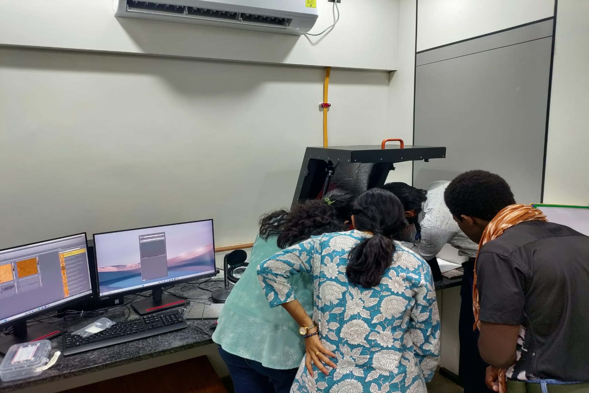
Students in B.Pharm and related programmes have a growing intersection with nanotechnology through nanoparticle drug delivery, pharmaceutical surface characterisation, and nanomedicine. As participant Dr. Tularam Barot demonstrated in the MNRDC workshop, pharmacy researchers routinely need SEM and AFM for particle size analysis, tablet surface uniformity, and coating characterisation.
The M.Pharm Pharmaceutical Technology programme at Parul University directly covers drug delivery systems and formulation technology where nanoscale characterisation is increasingly standard.
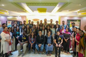
The MNRDC Advantage - Research Access That Defines Your Career
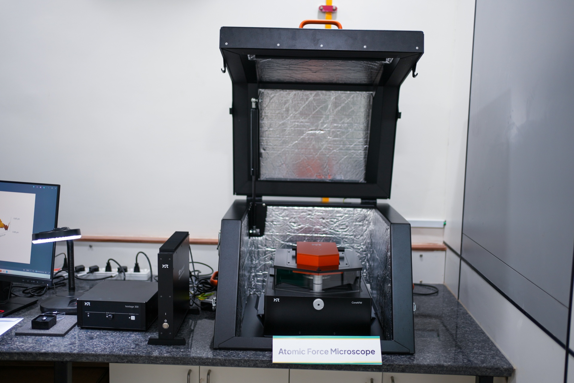
The single most career-differentiating factor for nanotechnology and materials science students is hands-on instrument access before graduation. A PhD scholar at a university without advanced characterisation facilities spends years waiting to access external labs – paying per sample, waiting weeks, and never developing the deep operational proficiency that comes from regular, supervised instrument time. At Parul University, the MNRDC’s 10-instrument portfolio – including the Rs.1.9 crore Hitachi SU3800 SEM, Bruker D6 PHASER XRD, and Nanosurf Core AFM – is accessible to enrolled researchers and PhD scholars as part of the university’s research infrastructure.
The MNRDC’s active funded projects – with ISRO, CSIR, and the Royal Academy of Engineering UK – create research opportunities that connect students directly to the priorities of India’s most important research-funding bodies. PhD scholars working on the ISRO Shape Memory Alloy project, the CSIR metamaterial antenna project, or the Royal Academy green hydrogen project graduate with publication records, ISRO/CSIR project experience, and instrument proficiency that positions them distinctively for both industry and academia.
Job Roles and Career Pathways
Entry-level characterisation scientists with SEM/XRD/AFM proficiency earn Rs.5-8 lakh per annum. Nanotechnology researchers at CSIR national laboratories earn Rs.7-15 lakh per annum at entry-to-mid level. Aerospace materials engineers at ISRO, DRDO, and HAL operate at the intersection of space technology and advanced materials. Green hydrogen researchers at PSUs implementing the National Green Hydrogen Mission (NTPC, ONGC, BHEL) represent a growing new career category with significant salary growth expected as the mission scales.
What 12th Grade Students Should Do Right Now
PCM students interested in nanotechnology should identify universities with genuine instrument access – not just laboratory infrastructure listed in brochures, but active testing facilities with published sample counts, external user programmes, and funded research projects. The MNRDC at Parul University publishes its sample counts (897+ SEM, 600+ XRD, 145+ AFM), its industry client list (60% repeat clients), and its funded projects on its official website. These are the metrics that distinguish research infrastructure from research marketing.
Prospective students can explore all undergraduate and postgraduate programmes at Parul University, or contact the admissions team directly through the university homepage. Take your research further with doctoral and postdoctoral programmes designed to maximise your academic potential.
FAQs
What is the best course to study for a nanotechnology career after 12th in India?
For engineering-focused nanotechnology careers: B.Tech Mechanical Engineering, B.Tech Chemical Engineering, or B.Tech Electronics and Communication Engineering. For research-oriented careers: B.Sc Physics followed by M.Sc Physics or M.Tech in a relevant specialisation. The most important factor beyond the programme is the research infrastructure available - specifically access to SEM, XRD, and AFM for hands-on characterisation training during your degree.
What is the salary for a nanotechnology researcher in India?
Entry-level materials characterisation scientists with SEM/XRD/AFM proficiency at semiconductor companies earn Rs.5-8 lakh per annum. CSIR national laboratory scientists earn Rs.7-15 lakh at entry-to-mid level. ISRO and DRDO engineers earn Rs.7-12 lakh at entry level with significant growth tied to research output. Academic faculty positions in nanotechnology at NAAC A++ institutions begin at Rs.8-15 lakh. PhD qualification and instrument proficiency significantly accelerate progression in all these tracks.
Is Parul University good for nanotechnology research?
Parul University houses the MNRDC - one of Gujarat's most comprehensively instrumented university-level material characterisation facilities, funded by the Government of Gujarat (Rs.1.49 crore), with active projects funded by ISRO, CSIR, and the Royal Academy of Engineering UK. The MNRDC operates a Rs.1.9 crore Hitachi SU3800 SEM (897+ samples), Bruker D6 PHASER XRD (600+ samples), and Nanosurf Core AFM (145+ samples) accessible to enrolled researchers. Parul University is NAAC A++, NIRF Top 50 Innovation, and QS Diamond Rated (Gujarat's first private university).
What is the scope of nanotechnology in India in 2026?
Nanotechnology scope in India is expanding rapidly across four fronts: semiconductor manufacturing (India Semiconductor Mission, Rs.76,000 crore incentive), green hydrogen (National Green Hydrogen Mission, 5MT/year target by 2030), space materials (ISRO's Gaganyaan, lunar programme, satellite expansion), and 5G/6G communications (CSIR-funded metamaterial antenna research for beyond-5G systems). All four domains require materials scientists, characterisation specialists, and thin film engineers - making 2026 an excellent entry point for nanotechnology careers.