Modern industries do not run on iron and plastic. They run on materials designed at the nanometre scale, sensors that detect environmental conditions in real time, and the engineering capability to synthesise new materials from first principles.
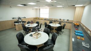
The Material Synthesis Zone inside Parul University’s Lakshya 2047 Centre for Future Skills, inaugurated by Union Minister Dr. Jitendra Singh on 8 May 2026, exists to develop this materials engineering capability at university level. The lab focuses on nanotechnology and sensor engineering, with research-grade equipment including a Techinstro Hydrothermal Autoclave, an indigenous DC Plasma System, a HOLMARC UV laser writing system, an Apex EZspin spin coater, an Autolab electrochemical workstation, an Ossila Four-Point Probe, and the broader microscopy and analytical infrastructure that serious materials research requires. The lab issues ASM International Materials Engineering and IEEE Sensors and IoT certifications.
Why materials engineering and sensor engineering matter at industrial scale
Look at any modern product. The performance that distinguishes good products from average ones is almost always materials-driven, often at the nanometre scale. Scratch-proof lenses for spectacles depend on materials science to deliver the hardness that prevents abrasion without sacrificing optical clarity. Energy storage devices depend on electrode materials engineered to maximise charge density and cycle life. Fresh fruit preservation depends on nanomaterial coatings that protect against bacteria and oxidation. IoT sensors depend on materials that can detect specific environmental parameters with reliability. Across consumer products, industrial systems, healthcare devices, and emerging technologies, materials engineering is the substrate that everything else builds on. The Material Synthesis Zone exists to produce graduates capable of doing this kind of work.
Also Read: PLC & SCADA Lab at Lakshya 2047 – Centre for Future Skills, Parul University!
The research-grade equipment inside the lab
- Techinstro Hydrothermal Autoclave. A heavy stainless-steel chamber connected to an electric motor and digital control panel, capable of synthesising nanomaterials within liquids through high pressures up to 100 bars and temperatures up to 300°C. The system features a built-in stirrer for tight temperature and pressure control, with typical runs of 8 to 10 hours to convert raw materials into nanomaterials. The lab also includes an automatic autoclave from Sailab Instruments for different types of high-pressure sterilisation and processing.
- Indigenous DC Plasma System. A homemade machine that uses ionised gas (plasma, the fourth state of matter) to transform the chemical composition of materials into something entirely different. The indigenous Plasma Generator signals the lab’s technical depth: building rather than buying complex equipment requires the kind of capability that distinguishes serious research environments. Applications include agricultural research and biomaterial surface activation.
- HOLMARC LWS-UV-T laser writing system for photolithography. A high-precision machine using a 405 nm laser to engrave microscopic circuits on materials. Used to create micro-electromechanical systems (MEMS) and semiconductor devices, the system extends the lab into the upstream of integrated circuit fabrication. Students gain hands-on experience with the kind of photolithography that the broader semiconductor industry depends on.
- Apex EZspin-PR spin coater. A high-speed device that rapidly rotates glass or silicon samples up to 8000 RPM, evenly coating them with an ultra-fine layer of liquid film. Spin coating is a foundational technique for thin-film deposition, used across semiconductor manufacturing, optical coatings, and sensor production.
- Autolab PGSTAT204N electrochemical workstation. Provides the electrochemical analysis infrastructure for studying electrode behaviour, battery research, biosensor development, and the broader range of electrochemical phenomena that energy storage and sensor research depend on.
- Ossila Four-Point Probe. Specialised instrument for measuring the electrical resistivity of materials, particularly thin films and semiconductors. Essential for characterising new materials and verifying that synthesised samples have the expected electrical properties.
- Tube Furnace with controlled gas atmospheres. Allows experiments to be conducted in the absence of oxygen or in specific controlled atmospheres. Critical for materials that react with oxygen during processing and for synthesis pathways that require inert or reducing environments.
- Microscopy and analytical instrumentation. Supporting equipment for characterising synthesised materials, including the imaging and analytical tools that let students verify what they have actually produced.
The three operational zones of the lab
The lab is divided physically into three zones to keep different kinds of work separate and safe:
- Processing zone. Where the actual synthesis happens: the Hydrothermal Autoclave runs, the DC Plasma System operates, the spin coater spins, the laser writing system engraves. The zone is configured for the active material-production work.
- High-temperature zone. Where furnaces and other thermal equipment operate. Separated from the rest of the lab because of the thermal load and the safety considerations that high-temperature work requires.
- Analytical and measuring stations. In the most stable part of the lab, with vibration isolation for instruments like balances, viscometers, pH meters, the Four-Point Probe, and the electrochemical workstation. Stability matters because vibration from the processing equipment (centrifuges, hydraulic presses) can otherwise contaminate analytical measurements.
The two certifications: ASM International and IEEE
- ASM International Materials Engineering Certification. Issued by ASM International, the principal global standards body for materials engineering. The credential demonstrates competence in materials engineering work across the breadth of disciplines that materials science covers, from metallurgy through polymers through ceramics through composites.
- IEEE Sensors and IoT Certification. Issued by the IEEE, demonstrating competence in sensor engineering and the integration of sensors with Internet of Things infrastructure. The credential is particularly relevant for graduates entering the sensor industry, IoT product development, and the broader smart-systems engineering space.
Both credentials are issued by global standards bodies, verified through their credential systems, and recognised by employers in the materials engineering, semiconductor, sensor, and IoT industries globally. Through the Lakshya 2047 Centre’s partnership architecture, both credentials also carry NSDC alignment inside India’s National Skills Qualifications Framework.
Cross-disciplinary use: who actually works inside the lab
- Physicists and chemists. The primary research users. They use the Hydrothermal Autoclave, high-temperature furnaces, and Ossila Four-Point Probe to manufacture and test raw nanoparticles, particularly for work in energy storage and spintronics.
- Bioscience, food technology, and agricultural researchers. Use the DC Plasma System, Laminar Air Flow, and Autolab Potentiostat for work on extending fruit lifespan, ensuring proper seed germination, lowering water pH, and developing biosensors.
- Electronics and Communication Engineering students. Use the photolithography and thin-film deposition infrastructure for sensor and MEMS device work.
- Mechanical Engineering students. Engage the lab for materials selection in mechanical design contexts, particularly where novel materials open new design possibilities.
- Postgraduate and PhD researchers. Use the lab for thesis work and funded research projects, particularly in nanotechnology, energy materials, biosensors, and applied materials engineering.
Career pathways the Material Synthesis Zone opens
- Materials Engineer. The foundational role. Materials Engineers work across consumer products, electronics, aerospace, automotive, energy, and industrial sectors. Hiring demand is structural because every product industry needs materials competence.
- Nanotechnology Researcher. Specialised role in research institutions, semiconductor companies, and emerging-technology firms. Postgraduate and PhD-track students with hands-on synthesis experience are positioned for these roles.
- Sensor Engineer. Designs and develops sensors for IoT applications, industrial monitoring, medical devices, and environmental sensing. The IEEE Sensors and IoT credential is directly aligned with this career pathway.
- Biosensor Researcher. Combines materials engineering with biological systems for medical diagnostics, food safety, and environmental monitoring applications.
- Energy Storage Specialist. Battery research, supercapacitor development, and the broader energy storage industry hire materials engineers with electrochemical workstation experience.
- Semiconductor Materials Engineer. The intersection of materials science and semiconductor industry, particularly relevant as India’s Semiconductor Mission expands and the materials side of the semiconductor supply chain becomes a national priority.
How the Material Synthesis Zone connects to other Lakshya 2047 labs
The lab pairs with the VLSI Lab for students working at the intersection of materials engineering and semiconductor chip design. Together, the two labs cover both the materials side and the design side of semiconductor work. The lab also intersects with the AICTE IDEA Lab Prototyping Zone for students integrating their synthesised materials into prototyped devices, and with the Mind Lab for research-grade students developing biosensors for cognitive and biomedical applications.
Parul University’s parallel Micro-Nano Research and Development Center (MNRDC) provides complementary research infrastructure for biotechnology and nano-scale materials work, with the Material Synthesis Zone serving as the Lakshya 2047 entry point for students who want to engage with this broader institutional research ecosystem.
FAQs
What kinds of materials do students actually synthesise in the lab?
Students synthesise a range of advanced materials depending on their project focus. Nanomaterials are produced through the Hydrothermal Autoclave for energy storage research, battery electrode work, and supercapacitor development. Thin-film coatings are produced through spin coating for optical applications, scratch-resistant surfaces, and electronic device fabrication. Surface-modified materials are produced through DC Plasma System processing for biosensor development, agricultural applications including seed treatment, and biomaterial surface activation. MEMS and semiconductor device patterns are produced through the UV laser writing photolithography system. The breadth of synthesis capability is what makes the lab a research-grade facility rather than a teaching-only infrastructure.
Which Parul University programmes access the Material Synthesis Zone?
Multiple Science and Engineering programmes engage the lab. Physics and Chemistry students from the Faculty of Applied Sciences are the primary research users. B.Tech in Electronics and Communication Engineering students engage for sensor and MEMS work. Bioscience, food technology, and agricultural researchers use the lab for biosensor development and food preservation research. B.Tech in Mechanical Engineering students engage for materials selection in mechanical design. Postgraduate and PhD researchers across multiple disciplines use the lab for thesis work and funded research projects.
What is special about the indigenous DC Plasma System in the lab?
The DC Plasma System inside the lab is indigenous, meaning it was built rather than purchased. Having an indigenous Plasma Generator system signals the lab's technical capability: building complex research equipment requires the kind of engineering depth that distinguishes serious research environments from teaching-only facilities. The plasma system uses ionised gas (plasma, the fourth state of matter) to transform the chemical composition of materials into something entirely different, with applications in agricultural research and biomaterial surface activation. The indigenous build is also one of the institutional Atmanirbhar Bharat operational examples inside the Lakshya 2047 Centre, demonstrating domestic capability for advanced research infrastructure.
What certifications can students earn through the Material Synthesis Zone?
Two globally recognised credentials. ASM International Materials Engineering Certification is issued by ASM International, the principal global standards body for materials engineering, and demonstrates competence across the breadth of materials science disciplines. IEEE Sensors and IoT Certification is issued by the IEEE, the international standards body for electrical and electronics engineering, and demonstrates competence in sensor engineering and IoT integration. Both credentials are recognised by employers in materials engineering, semiconductor, sensor, and IoT industries globally, and both carry NSDC alignment inside India's National Skills Qualifications Framework through the Lakshya 2047 Centre's partnership architecture.
How does the Material Synthesis Zone teach students to work confidently with advanced equipment?
The lab's training emphasises hands-on use without fear of failure as the foundational learning principle. If a material does not form correctly in the furnace or spin coater, students alter the parameters and try again. The iterative-attempt approach develops the experimental confidence that serious research work requires, without the costly mishaps that would result from students arriving at industrial labs without prior hands-on experience. Months of practical experiments on the UV Laser Writing System, the DC Plasma System, and the broader equipment set develop the experimental skills that the materials and sensor industries actively recruit for. The fear-elimination training is part of what makes the lab a research incubator rather than just a teaching facility.