Lakshya 2047 at Parul University is bifurcated into three groups. These labs will prepare the students for the future demands by offering courses that match not only the present requirements but also the coming technological advancements. The NSDC Lab Ecosystem houses ten certification-aligned global-vendor laboratories (Apple Lab, AR/VR Lab, ABB Lab, NVIDIA Lab, Cisco Lab, AWS Lab, VLSI Lab, ANSYS Lab, Adobe Lab, Autodesk Lab) delivering global certification training integrated with university curriculum. The AICTE AVPL/IDEA Lab Zone houses drone training, fabrication centres, material synthesis, and teamwork spaces. The third grouping is the research-laboratory cluster, which houses the Centre of Excellence in Sensor Technology alongside the Mind Lab and the Special Integrated Facilities Idea Lab supported by AICTE.
The structural distinction matters. The NSDC Lab Ecosystem is skill-certification infrastructure: students train against global certification programmes integrated into the existing B.Tech curriculum. The research-laboratory cluster, where the Sensor Lab sits, is research infrastructure: faculty and Ph.D. candidates produce patents, peer-reviewed publications, and applied research collaborations from this space. The Centre of Excellence in Sensor Technology is one of the most output-intensive nodes in this research cluster. The Mind Lab operates as an adjacent research environment within the same cluster. Full lab-by-lab structure is documented in the Lakshya 2047 lab catalogue.
What a Centre of Excellence in Sensor Technology actually does
The apps on phones or on other devices and the smart tech at homes work because they have sensors in them. Almost every device, like medical, environmental monitoring, etc., works with sensors in them. Making and improving the sensors is the foundational work for a smart, intelligent technology ecosystem in India’s vision 2047. The Centre of Excellence in Sensor Technology at Parul University works across three sensor classes: electrochemical sensors that detect specific ions, gases, and biochemical species; optical sensors that respond to light, fluorescence, or spectral signatures; and biosensors that combine a biological recognition element with a transducer to detect proteins, DNA, glucose, or pathogens.
- Electrochemical sensors: ion-selective electrodes, gas sensors, glucose biosensors, heavy-metal detection arrays.
- Optical sensors: fluorescence-based detection, surface plasmon resonance configurations, colourimetric assays.
- Environmental sensors: VOC detectors, particulate matter sensors, water-quality monitoring arrays.
- Biosensors: enzyme-based, antibody-based, aptamer-based, and DNA-based recognition systems.
The instruments inside the Sensor Lab
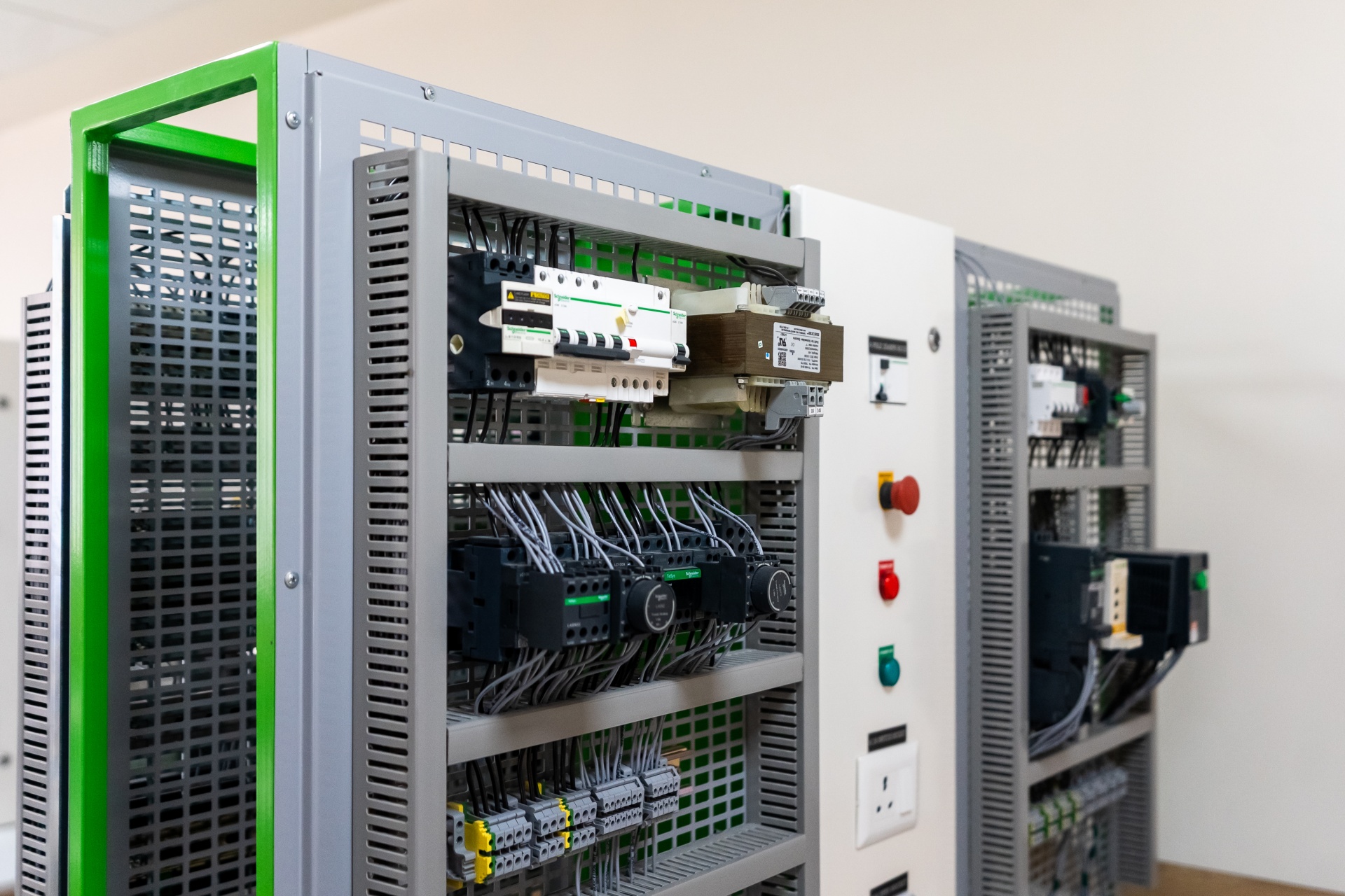
The instrument suite at the Centre of Excellence in Sensor Technology is designed to support sensor development from material synthesis through device fabrication to electrochemical characterisation. Each instrument anchors a different stage of the research pipeline. The lab operates in scope-adjacency to the Micro Nano Research and Development Center (MNRDC) at Parul University, where SEM, XRD, AFM, and tribology characterisation services are housed.
Read More: Lakshya 2047 Inauguration at Parul University.
Autolab PGSTAT204N potentiostat
The Autolab PGSTAT204N is the lab’s central electrochemical measurement workstation. It controls and measures electrical conditions at the electrochemical interface where electrons transfer between electronic and ionic conductors. The specifications place it in the research-instrument category rather than the teaching-equipment category.
- Potential range: ±10V.
- Compliance voltage: ±20V.
- Accuracy: ±0.2%.
- Use cases: electrochemical sensor development, energy storage research, corrosion studies, electrocatalysis characterisation.
The career value of mastering this instrument is substantial. Pharmaceutical companies developing electrochemical drug delivery systems, battery manufacturing plants working on next-generation chemistries, corrosion engineering firms, and medical diagnostics development companies all hire researchers who can run a potentiostat at this level.
Metrohm Dropsens 220BT electrochemical analyser
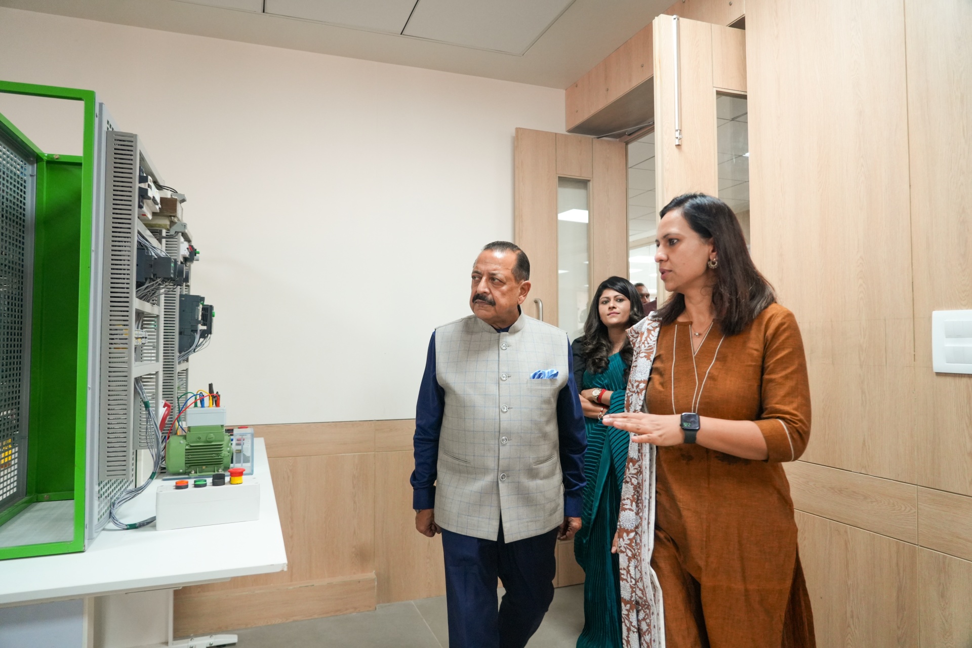
Dr. Jitendra Singh observed the Metrohm Dropsens 220BT closely during the walkthrough. The instrument is a portable, Bluetooth-enabled electrochemical analyser that allows electrochemical measurements to be performed outside the laboratory environment. This portability matters: it makes field deployment of sensor research feasible, which is the difference between a sensor that works in a lab and a sensor that works in a hospital, a river, or a factory floor.
Ossila Four Point Resistance Probe System
The Ossila Four Point Resistance Probe System characterises surface coatings and thin-film electrical properties using sheet resistance as the measurement standard. The measurement range covers 100 milliohm per square at the conductive end to 10 megaohm per square at the resistive end. Anyone working on thin-film electronic components, organic solar cells, transparent conductors, nanomaterial coatings, or two-dimensional materials such as graphene needs this system. Students pursuing the M.Tech in Nanotechnology use this instrument across their thesis projects.
Spin Coater
The spin coater is a process where uniform thin films are placed onto the flat substrate, which is spun at a controlled pace. Balancing the speed of the spin with the liquid solution properties, films can be created to suit the requirements. It can deposit films from a few nanometers to several micrometers thick. The technique is foundational for sensor fabrication, organic electronics, and photovoltaic device development. A research student fabricating a glucose biosensor will spin-coat the enzyme layer onto the working electrode. A student building an organic solar cell will spin-coat the active layer onto a transparent conductor.
UV Laser Writing System
Imagine you are drawing on a hair strand and you realise that your pen is seven times thinner than that. The UV Laser Writing System has this precision, which uses a 405-nanometer fibre-coupled laser focused to s spot smaller than ten micrometers to write microscopic patterns for photolithograpgy. This enables fabrication of MEMS devices, microfluidic chips, and semiconductor test structures. The dimensions the system can reach move student research capability into the size scales that the most advanced technology sectors operate at.
Hydrothermal Autoclave
The Hydrothermal Autoclave is a sealed pressure reactor rated to 100 bar and 300°C. It synthesises high-quality nanoparticles and advanced materials under conditions that accelerate reactions impossible at room temperature. Metal oxide nanoparticles, quantum dots, nanowires, and porous framework materials can all be produced here with controlled properties. The autoclave is the source material factory for sensor research: where the functional sensing materials themselves are created before they are deposited, characterised, and integrated into devices.
DC Plasma System
The DC Plasma System generates plasma, ionised gas with extreme chemical reactivity, for etching, cleaning, and activating material surfaces. The system is foundational for semiconductor manufacturing, thin-film deposition, surface engineering, and biomedical device fabrication. Skills developed on this instrument map onto the VLSI and semiconductor industry that India’s B.Tech in Electronics with VLSI Design specialisation feeds into.
CNC Machine for Substrate Fabrication
A CNC machine for precision carving sits inside the Sensor Lab specifically for manufacturing custom sensor substrates and microfluidic structures on-site. The advantage of having fabrication adjacent to characterisation is the speed of the design-iterate-test cycle. A student who notices a problem with a sensor housing geometry can redesign, fabricate, and re-test on the same day.
Patents and what they signal
More than thirty patent applications were disclosed on the walkthrough display panels. Patents are the most rigorous publicly verifiable evidence of research output in any technology institution. They survive peer review, prior-art search, and formal examination at a national patent office. A research-intensive Centre of Excellence with thirty-plus disclosed patent applications operates at a different level from a teaching lab. Parul University holds NAAC A++ accreditation at a 3.55 CGPA, documented in the Foundation Day account, and is recognised by DSIR under the Ministry of Science and Technology, with a DST-funded research footprint of ₹58.31 crore in active government grants and ₹4.37 crore in private-funded engagements across 315 funded projects.
What students build here, and where they go after
The Sensor Lab is open to students across the engineering and applied sciences programmes that touch sensor technology. The B.Tech in Electronics and Communication Engineering sends students here for sensor circuit design and signal conditioning work. The B.Tech in Biotechnology sends students for biosensor research projects. The M.Tech in Nanotechnology runs full thesis cycles here. The Ph.D. in Engineering and Technology candidates anchor their long-form research programmes against the lab’s instrument suite.
- Research-output career paths: sensor design engineer at automotive and aerospace OEMs, biosensor developer at medical diagnostics firms, materials characterisation specialist at semiconductor companies.
- Applied-engineering paths: IoT product engineer at smart-building and smart-city integrators, instrumentation engineer at process industries, MEMS engineer at chip-design startups.
- Academic and policy paths: Ph.D. researcher at IITs, NITs, IISc, and international universities; research programme officer at DST, DBT, and CSIR labs.
- Entrepreneurial paths: founder of a sensor startup incubated through PIERC, the Parul University start-up incubator with 254 incubated startups.
Read More: 19 cities, 280 companies, 100+ International Professors at Parul University.
How the Sensor Lab connects to the wider MNRDC ecosystem
Sensor research and material characterisation are not separable disciplines. A new sensor material needs to be imaged, structurally characterised, and surface-mapped before its properties can be understood. The Sensor Lab at Lakshya 2047 produces and tests electrochemical and optical sensor devices. The Micro Nano Research and Development Center, located in scope-adjacency, provides the structural and morphological characterisation that sensor research depends on.
- Scanning Electron Microscopy: imaging and elemental composition of sensor surfaces via the SEM-EDS facility.
- X-Ray Diffraction: crystalline phase identification using the D6 Phaser.
- Atomic Force Microscopy: surface roughness and nano-imaging at the AFM characterisation facility.
- Tribology: wear, friction, and surface durability via the pin-on-disc tribometer facility.
External researchers, industry partners, and Ph.D. candidates from other institutions can also submit samples to the Micro Nano Research and Development Center for paid testing services. Sample submission protocols, size limits, and rejection criteria are documented in the MNRDC sample submission guide. The Sensor Lab and MNRDC together constitute a research backbone unusual in scope for a single private university in India.
FAQs
What is the Centre of Excellence in Sensor Technology at Parul University?
The Centre of Excellence in Sensor Technology is a research-intensive sensor and biosensor development laboratory at Parul University, Vadodara, housed inside the Lakshya 2047 Centre for Future Skills (Gujarat's first NSDC Centre for Future Skills established in partnership with the National Skill Development Corporation and Ethnotech Academy). It is fitted with the Autolab PGSTAT204N potentiostat, the Metrohm Dropsens 220BT portable Bluetooth electrochemical analyser, the Ossila Four Point Resistance Probe System, a spin coater, a 405 nm UV laser writing system, a hydrothermal autoclave rated to 100 bar and 300°C, a DC plasma system, and a CNC machine for substrate fabrication.
Is the Sensor Lab at Parul University part of the NSDC Lab Ecosystem?
No. The Centre of Excellence in Sensor Technology at Parul University sits in the research-laboratory cluster at Lakshya 2047, alongside the Mind Lab and the Special Integrated Facilities Idea Lab supported by AICTE. The NSDC Lab Ecosystem is a separate structural grouping covering ten certification-aligned global-vendor laboratories (Apple, AR/VR, ABB, NVIDIA, Cisco, AWS, VLSI, ANSYS, Adobe, Autodesk). The Sensor Lab is research infrastructure rather than skill-certification infrastructure: it produces patents, peer-reviewed publications, and applied research output.
How many patents has the sensor lab at Parul University produced?
More than thirty patent applications were on display from the Centre of Excellence in Sensor Technology at Parul University during the Lakshya 2047 inauguration walkthrough on 8 May 2026, alongside more than fifty distinct sensor types. The patent applications cover electrochemical sensors, biosensors, optical sensors, and environmental monitoring devices developed by research faculty and Ph.D. candidates.
Can external researchers and industry use the sensor lab at Parul University?
The Centre of Excellence in Sensor Technology serves Parul University students, faculty, and Ph.D. candidates first. Adjacent characterisation services through the Micro Nano Research and Development Center, including SEM, XRD, AFM, and tribology testing, are open to external researchers and industry on a paid sample-submission basis. Submission protocols, size limits, and acceptance criteria are documented at MNRDC.
Which programmes at Parul University use the Centre of Excellence in Sensor Technology?
The Centre of Excellence in Sensor Technology serves the B.Tech in Electronics and Communication Engineering, the B.Tech in Biotechnology, the M.Tech in Nanotechnology, the M.Tech in VLSI Design, and the Ph.D. in Engineering and Technology at Parul University. B.Tech in Computer Science Engineering students working on IoT projects also access the lab for sensor integration work.